Welcome to IgMin Research – an Open Access journal uniting Biology, Medicine, and Engineering. We’re dedicated to advancing global knowledge and fostering collaboration across scientific fields.
Welcome to IgMin, a leading platform dedicated to enhancing knowledge dissemination and professional growth across multiple fields of science, technology, and the humanities. We believe in the power of open access, collaboration, and innovation. Our goal is to provide individuals and organizations with the tools they need to succeed in the global knowledge economy.
IgMin Publications Inc., Suite 102, West Hartford, CT - 06110, USA
The experimental team has developed a technology of step-by-step low-temperature diffusion doping of gadolinium and scandium into silicon that allows the clusters of impurity atoms to be uniformly distributed throughout the entire bulk of the silicon material. It was shown that, unlike the samples obtained under the high-temperature diffusion doping technology, in the samples obtained under the novel technology the team had detected any surface erosion or formation of alloys and silicide in the near-surface region. The authors have revealed increased thermostability and radiation resistance of silicon samples dotted with clusters of impurity atoms of gadolinium and scandium.
The authors have conducted comprehensive studies by using the techniques of tagged atoms, autoradiography, measurement of conductivity and Hall effect, isothermal relaxation of capacitance and current of diffusion, solubility, and electrophysical properties of scandium in silicon under various doping conditions and for a wide temperature range (1100 ÷ 1250 0С). Diffusion parameters, solubility and acceptor nature of scandium in silicon as well as thermal stability of silicon doped with gadolinium and scandium impurity atoms have been established.
In the fast-developing area of semiconductor physics of particular interest is the issue of engineering a novel type of materials by forming clusters on the surface and in the bulk of silicon that would allow changing its fundamental parameters. The development of a technology aimed at forming clusters of impurity atoms, that would make it possible to create nanosized structures in the silicon matrix with a sufficiently high concentration and given composition, structure, and physical parameters, is becoming one of the latest trends in microelectronics [11Egamberdiev BE. Electron spectroscopic studies of the physical properties of epitaxial combinations and ion-implanted layers in silicon. Doctoral dissertation. 2003; С 243.-1010Bagraev NG, Romanov VV. Magnetism of AIIIBV crystals doped with rare elements. FTP. 2005;39(10):1173-1182.].
Semiconductor materials with engineered structures throughout the entire bulk of the crystal, especially with clusters of impurity atoms, are of great scientific and practical interest. In such materials, a number of novel physical phenomena have been discovered that make a great contribution to the development of modern microelectronics and nanoelectronics. In this regard, of particular interest is the issue of forming clusters of impurity atoms of rare earth elements in silicon [1111Abdurakhmanov BA, Egamberdiev BE, Iliev KhM, Tachilin SA, Toshev AR. The influence of silicon-germanium microheterojunctions on the parameters of silicon solar cells. J Electron Mater Process. Moldova. 2010;(5):124-126.-2222Fistul VI. Atoms of dopant impurities in semiconductors. Moscow: Fizmatlit; 2004; 432.].
The present study is partially motivated by the existence of a number of unresolved issues from the point of view of developing a technology for the formation of clusters of impurity atoms of rare earth elements with a controlled structure and properties in the silicon lattice that still remains one of the urgent and promising problems of modern nanoelectronics.
The creation of clusters of impurity atoms of rare earth elements in silicon makes it possible not only to control the fundamental parameters of silicon, and its magnetic properties, but also reveals a number of yet unknown physical phenomena in silicon. Application of such phenomena would open up new possibilities for creating device structures with unique technical characteristics
By implementing the technique of microprobe analysis (Jeol Super Probe JXA-8800 R/RL), IR microscopy (INFRAM-I), and AFM (Dimension 3000) the experimental team studied the process of forming clusters of atoms of gadolinium and scandium, as well as changes in their structure, size, and density. The electrical parameters of the samples were measured using the four-probe method and the Hall Effect technique. Based on theoretical calculations, the authors have determined the concentrations of impurity atoms participating in cluster formation.
The state of impurity atoms of gadolinium and scandium in the bulk of the silicon crystal lattice was studied using an infrared microscope INFRAM-I. The INFRAM-I infrared microscope observes not only the surface of a silicon sample but also practically all its layers, i.e., allowing it to examine the sample throughout its entire bulk.
To measure the lifetime of minority charge carriers, the technique of transient processes of a sinusoidal current of large amplitude was used. The choice of this technique was motivated by the fact that the Si<P, Gd> and Si<P, Sc> samples, as well as the reference samples, had changed their resistivity in a fairly wide range during heat treatments. Therefore, the use of standard pulse methods made it difficult to obtain reliable information. The measurement error was in the range of more than 5%.
Phosphorus-doped and boron-doped single-crystalline silicon samples of both n- and p-type conductivity, grown by the Czochralski technique (concentration of residual oxygen was in the range of 6*1017 cm-3, resistivity in the range ρ~1 ÷ 100 Ohm×cm) were taken as reference samples. The thickness of the original silicon samples was 380 µm. Gadolinium and scandium were used as dopant elements. Doping of the samples was carried out in evacuated quartz ampoules from a thin metal layer deposited in a vacuum on the surface of silicon samples. Reference silicon samples (without gadolinium and scandium atoms) were annealed in separate ampoules under similar conditions in order to evaluate the effect of diffusion doping on the electrical parameters of the samples. Mechanical and chemical processing of all samples was carried out under identical conditions.
To study the silicon doped with scandium, the samples were prepared as follows. For electrophysical studies, diffusants happened to be stable isotopes of metallic scandium or salts of trivalent scandium chloride. A metal layer of the scandium radioactive isotope 46Sc was deposited on the surface of n-type silicon with a resistivity ρ= 15 Ω ·cm or a layer was deposited from a solution of scandium chloride labeled with the radioactive isotope 46Sc.
Diffusion doping was carried out on open air, in evacuated quartz ampoules (~ 10-5 10-7 mmHg), as well as in evacuated ampoules in argon atmosphere in the temperature range of 1100÷12500С. The duration of diffusion doping varied depending on the diffusion temperature from 5 to 72 hours. After diffusion doping, the samples were repeatedly washed in hydrofluoric acid, aqua regia, and also in a boiling mixture of H2O2 : HCl. After that, the edges of the sample were etched down to a depth of ~100 µm, thus significantly exceeding the diffusion depth of ~ 10 µm.
The diffusant profile was determined by the method of sectioning, i.e., etching thin layers (in a solution of HF: HNO3 = 1:50 with the washing in a mixture of H2O2 : HCl) and measuring the residual activity of the sample. The residual activity of the sample was measured using a UMF-1500 M low-background unit with an SBT-11-type β-counter. Identification of 46Sc spectra was also carried out by means of measurements on an AI-1024-type pulse analyzer. The thickness of the removed layers (0.050.5µm) was determined by intermittent weighing of the sample. The autoradiograms obtained before and after doping, as well as during the removal of layers, indicate a uniform distribution of Sc impurities over the cross-section of the sample and the absence of embedded inclusions.
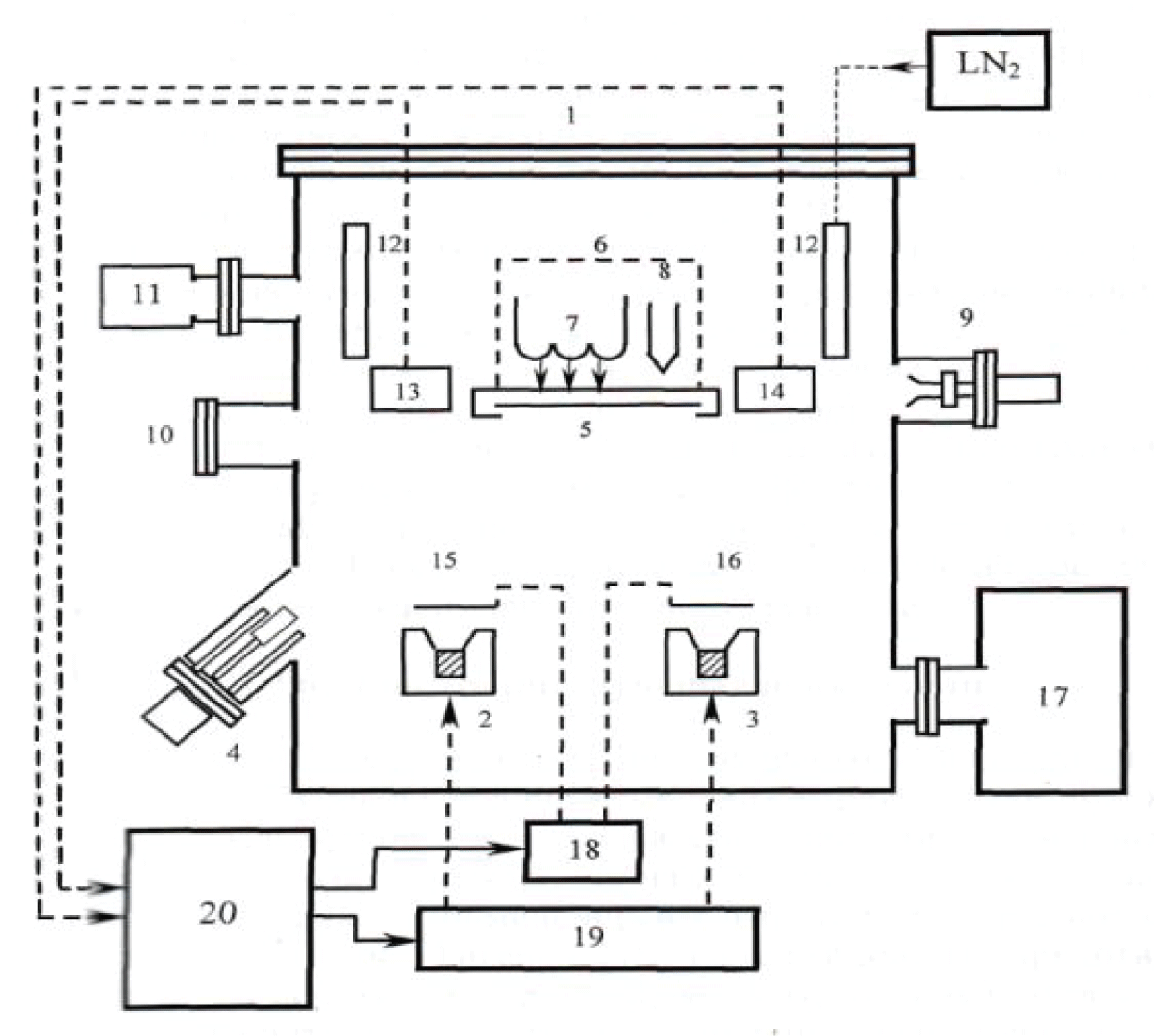
Figure 1 shows an analytical growth chamber was shown, where 1, 2, and 3 are electron-beam evaporators; 4-effusion source; 5-sample; 6-manipulator; 7-heater; 8-thermocouple; 9-electron gun of the fast electron diffractometer; 10-fluorescent screen; 11 - a quadrupole gas analyzer; 12-cryopanel; 13.14 - deposition rate sensors (quartz); 15,16 - dampers; 17-ion pump; 18-control dampers with a servo drive; 19-power supplies of electron-beam evaporators; 20 - processor unit.
Figure 1: Analytical growth chamber: 1, 2, 3 - electron beam evaporators; 4-effusion source; 5-sample; 6-manipulator; 7-heater; 8-thermocouple; 9-electron gun of the fast electron diffractometer; 10-fluorescent screen; 11 quadrupole gas analyzers; 12-cryopanel; 13, 14- deposition rate sensors (quartz); 15, 16 dampers; 17-ion pump; 18-control dampers with a servo drive; 19-power supplies of electron-beam evaporators; 20-processor unit.
The sample 5, mounted on a molybdenum holder, was placed inside the chamber on a manipulator 6. The manipulator was equipped with a heater 7 and a thermocouple 8, which made it possible to control the sample temperature in the temperature range from room temperature up to 10000С with an accuracy of ±0.5 0С. To ensure uniform heating of the sample and uniform deposition of evaporated materials, the holder with the sample was rotated using an electric motor.
The growth chamber was equipped with a reflection high-energy electron diffractometer, which made it possible to analyze the structure of the crystal surface directly in the course of growth. The diffractometer included an electron gun 9 and a luminescent screen 10.
Quadrupole gas analyzer 11 was used to control the composition of the residual gas atmosphere. The grown epitaxial structures were studied in the analytical chamber by Auger electron and secondary ion mass spectrometry. The vacuum in the system was maintained at the level of 5‧10-9 Pa.
Having investigated the clusters of impurity atoms of gadolinium and scandium, the authors have noted that this is not just a random accumulation of a certain number of atoms of some impurity somewhere in the lattice. This is a local region of a semiconductor enriched with impurity atoms, which, as a rule, is characterized by a clearly defined structure with an ordered arrangement of both impurities and the main atoms of the lattice. Impurity atoms in a cluster themselves enter a sublattice with a certain arrangement of atoms and ions, which is correlated with the semiconductor lattice, which explains their relatively high stability.
Under external influence, clusters of impurity atoms can change their state. The search for ways to control the state of clusters and their ordering in the crystal lattice of a semiconductor is of great scientific and practical interest. This is due not only to the chance of creating a bulk nanostructured semiconductor material but also to obtaining new types of photonic materials and bulk superlattices with specified parameters. The study of semiconductor materials with an ordered distribution of impurity atom clusters as a whole makes it possible to determine their unique functionality.
The essence of the “low-temperature diffusion doping” technique developed by us is as follows. The studied samples and diffusant are placed into evacuated quartz ampoules (pressure in the ampule ~10-6 mmHg). They are placed in a diffusion furnace at T=300K. It has been established in advance that the temperature of the furnace at the location of the ampoule gradually increases at a rate of 5 deg/min. Thereafter, the samples are heated to a temperature of T= (550 ÷ 700 0С) and kept at this temperature for t = (10 ÷ 20) min, then the furnace temperature is made to rise quickly (at the rate of 150 ÷ 200 deg/min) to a certain temperature (T=1200 ÷ 1250 0C) and at this temperature the samples are kept for a while, after which the ampoules are removed from the furnace and cooled at a rate of 2000/sec.
Based on the experimental results, it can be argued that at low temperatures, diffusion actually occurs via interstices, and impurity atoms are in interstitial states. An additional proof of this assumption can be the fact that at low-temperature diffusion, the calculated concentration of vacancies will be Nv~107 cm-3, i.e., almost 7-8 orders of magnitude less than the concentration of impurity atoms in the interstices.
One of the most important conclusions stemming from these experimental results is that the diffusion mechanism and the concept of solubility of impurity atoms under conditions of low-temperature diffusion differ significantly from diffusion at high temperatures, and the basic diffusion parameters and solubility obtained in this case require significant correction.
As the experiments showed, the new technology, in addition to the scientific novelty described above, has a number of important practical points alike: the diffusion process duration is reduced by 2 - 2.5 times, the power consumption for diffusion is reduced by 2 times, the formation of various alloys, silicide, both on the surface and in the near-surface area and surface erosion are almost completely eliminated. All the above advantages of the new method make it possible not only to simplify the technology of obtaining samples but also to form clusters of impurity atoms.
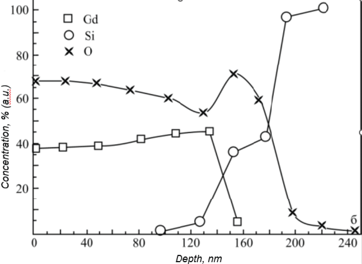
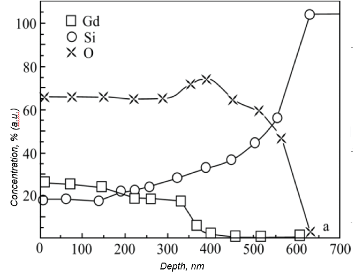
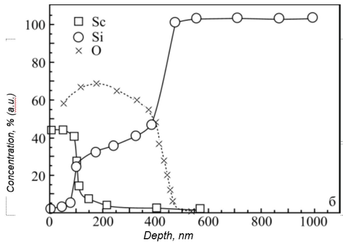
The concentration profiles of elements calculated by a special computer program designed for the analysis of the backscattering spectra of ions are shown in Figures 2-4. The concentration profiles of elements in “rear earth element-silicon” structures that have not undergone high-temperature annealing are shown in Figure 2.
Figure 2: Concentration profiles of Gd in silicon samples not subjected to high-temperature annealing.
Figure 3: Concentration profiles of Gd in silicon samples subjected to high-temperature annealing.
Figure 4: Concentration profiles of Sc in silicon samples subjected to high-temperature annealing.
From Figure 2 it can be seen that, in all structures, the concentration of rare earth elements in the film noticeably increases in the direction of the silicon boundary. This is applicable to all structures with rare earth elements obtained from a metal layer and is explained by the presence of metal at the interface with the substrate.
The concentration profiles of elements in structures that have undergone high-temperature annealing differ from the ones reflected in Figure 3.
Here, the concentration of rare earth elements gradually decreases towards the interface with silicon, which is explained by the escape of rare earth ions from the film into the silicon substrate due to diffusion. As a result, the shape of the spectrum of scattered neutrons also noticeably changes, where the peak of rear earth elements becomes lower and that of oxygen is slightly higher (Figure 4).
From the analysis of concentration profiles shown in Figure 3, it can be determined that the total thickness of the mixed oxide layer for such structures is from 0.1 to 0.6 µm, and the thicknesses of the rare earth layers are noticeably tinier from 0.05 to 0.1 µm, which corresponds to the thicknesses of the original layers of rare earth elements. At greater depths of silicon, the content of layers of oxygen-enriched and rare earth elements decreases.
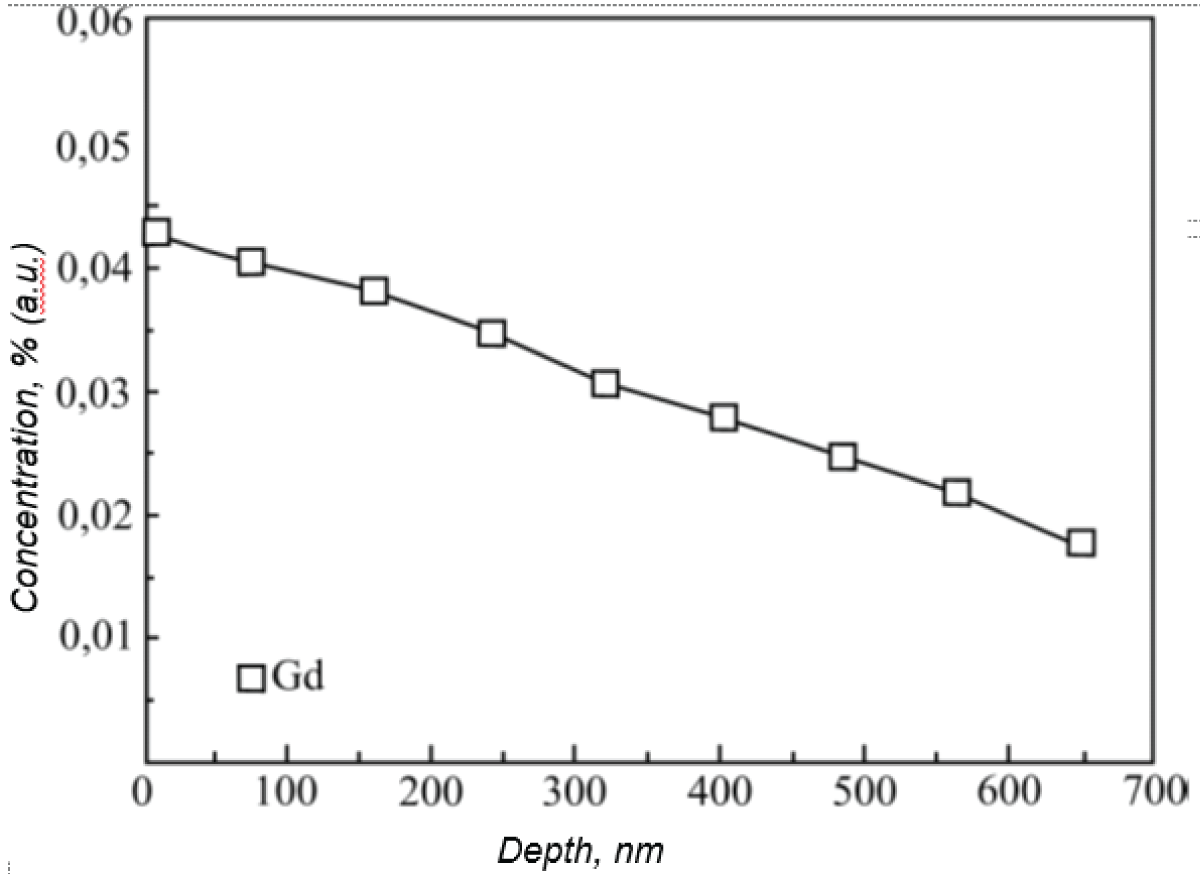
Figure 5 shows the concentration profiles of gadolinium in silicon after annealing at 12000C for 3 hours, measured on samples after removing all oxide layers. For the elements under consideration, the numerical values of the concentration in the surface layer of silicon with a thickness of 400 nm are more than 0.01% (at.), i.e., more than 1020 cm-3, which significantly exceeds the concentration of rare earth elements in silicon, usually achieved with diffusion doping.
Figure 5: Concentration profiles of Gd in silicon diffusion layers. Diffusion temperature 12000C, diffusion time 3 hours.
Hole concentration in all studied rare earth elements lies in the range from 1014 to 1017 cm3, that is, much less than the concentration of elements themselves. Thus, we can conclude that a significant proportion of rare earth elements is in a thin “tenth of a micrometer” silicon surface layer in an electrically inactive state.
In general, it was found that the total content of rare earth elements in the surface layers of silicon, according to elemental analysis, is quite high (up to 1020 cm-3), significantly exceeding concentrations that are usually obtained by diffusion of rare earth elements into silicon. At the same time, the concentration of electrically active acceptor impurities, determined from electrophysical measurements, is at least an order of magnitude lower (not exceeding 1019 cm-3). This implies that a significant portion of atoms of rare earth elements is discovered in the surface layer of silicon in an electrically inactive state.
Thus, the traditional mechanism of impurity diffusion via vacancies, which is usually used to explain the high-temperature diffusion of rare-earth elements into silicon, clearly does not take into account the entire behavior of a rare-earth impurity in silicon at high temperatures. Based on the analysis of the above experimental results, one may conclude that during high-temperature processing of silicon structures with films of rare earth elements on the surface, one of the dominant processes is the simultaneous diffusion of rare earth elements and oxygen from the rare earth elements-rich film into silicon, as evidenced by the rather high oxygen content in the surface layers of silicon. In this case, apparently, they interact with the formation of complexes in the crystal lattice of silicon. Another possible process may be the interaction of rare earth elements with silicon with the formation of a silicide or silicate phase, although X-ray analysis does not show the presence of such phases in appreciable amounts.
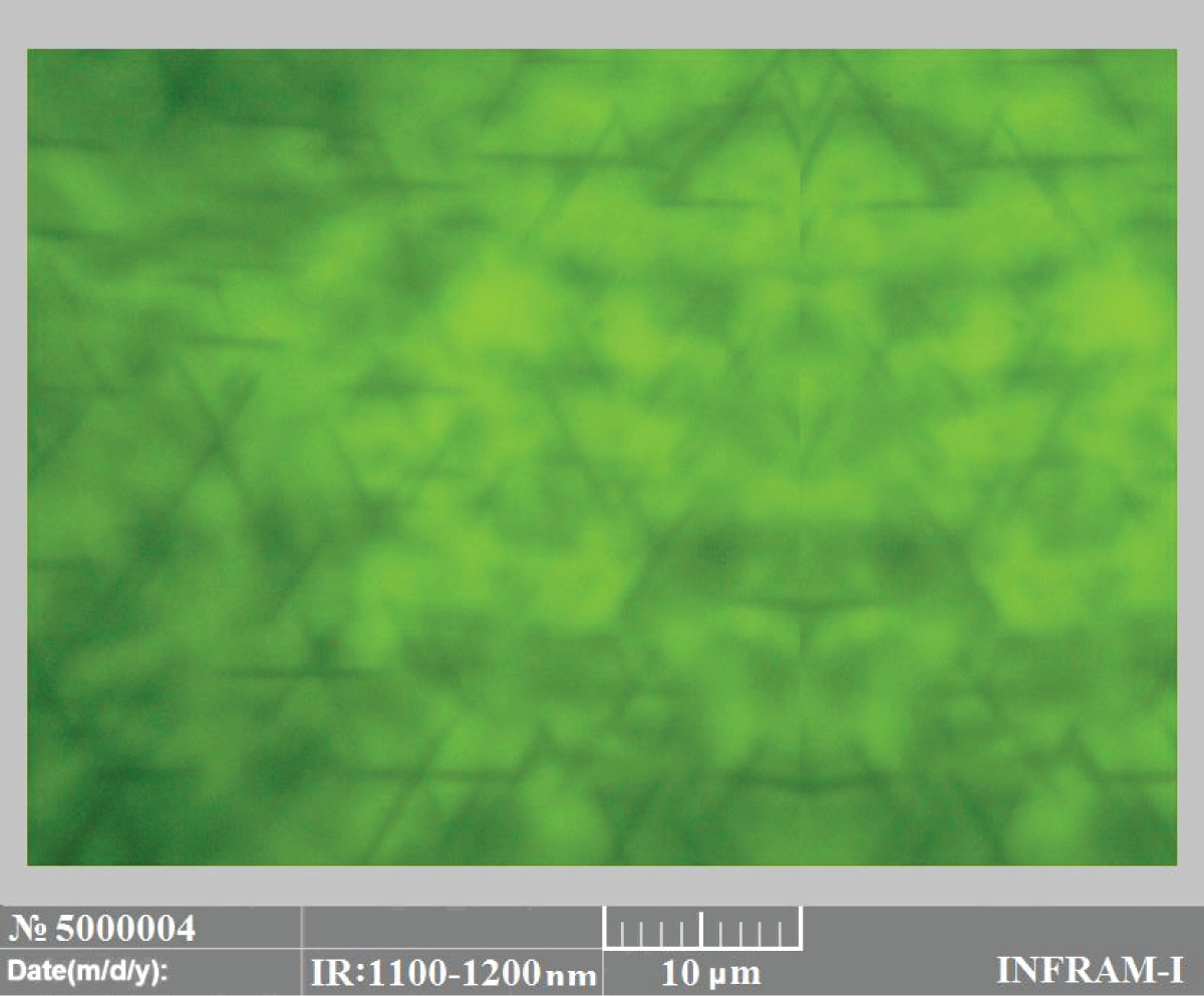
After polishing the surface of the samples, the state of clusters of gadolinium atoms was studied on an infrared microscope “INFRAM-I”. To make sure that the formation of clusters occurs throughout the entire volume of the crystal, the samples were subjected to step-by-step grinding, starting from the crystal surface to a depth (at 5 μm increments) to half the thickness of the sample, and each time the samples were again polished and investigated on an IR microscope.
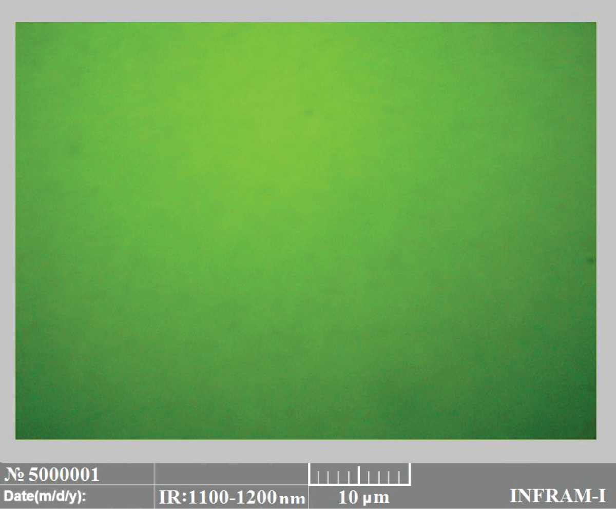
As shown by the results of IR microscopic studies in all samples, regardless of the type and concentration of the initial impurity atoms, uniformly distributed dark dots are observed, i.e., clusters of gadolinium atoms with a size of d=2 ÷ 15 μm. Figure 6 shows a micrograph of a silicon sample into which gadolinium was diffused using conventional high-temperature diffusion technology. As can be seen from the figure, in the sample doped with gadolinium applying to the traditional technique, the cluster formation does not occur at all.
Figure 6: Micrograph of the bulk of a silicon sample into which gadolinium was diffused using conventional high-temperature diffusion technology.
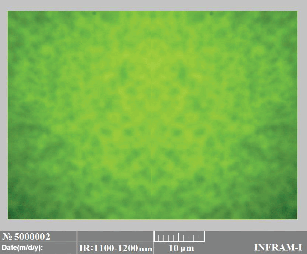
A micrograph of the surface of a silicon sample doped with gadolinium by staged low-temperature diffusion is shown in Figure 7.
Figure 7: Micrograph of a silicon sample doped with gadolinium by staged low-temperature diffusion.
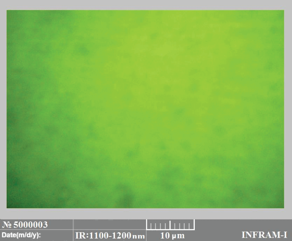
The authors have revealed that in the case of incremental-rise low-temperature diffusion, the temperature and time of diffusion affect not only the penetration depth of the impurity but also the size of clusters being formed. Moreover, it can also be a cause of failure to form those clusters. Figure 8 shows a photomicrograph of a silicon sample obtained by two-stage gadolinium diffusion at relatively low final temperatures and exposure times.
Figure 8: Micrograph of a silicon sample obtained by two-stage gadolinium diffusion at relatively low final temperatures and exposure time
As can be seen, the number of formed clusters is very small, and their sizes are also small, which are on the order of hundreds of nanometers. With a further increase in the number of diffusion stages, their duration, and temperature, large clusters of impurity gadolinium atoms several microns in size were obtained that were uniformly distributed over the entire bulk of the crystal. Quite interesting results were obtained with a three-stage diffusion doping technique. In this case, clusters were formed with the participation of lattice defects permanently present in the silicon crystal (Figure 9).
Figure 9: Micrograph of a silicon sample obtained by three-stage gadolinium diffusion at relatively high final temperatures and long exposure times.
It has been determined that, if a silicon sample has a thickness of about 380 µm, gadolinium penetrates to a depth of 60 µm, and the clusters allegedly form at the depth of 50 µm uniformly scattering throughout the thickness. The study of the effect of low-temperature annealing on the size and distribution of clusters showed that upon annealing in the temperature range of 6008000С, self-ordering and enlargement of clusters of impurity atoms of gadolinium are being observed.
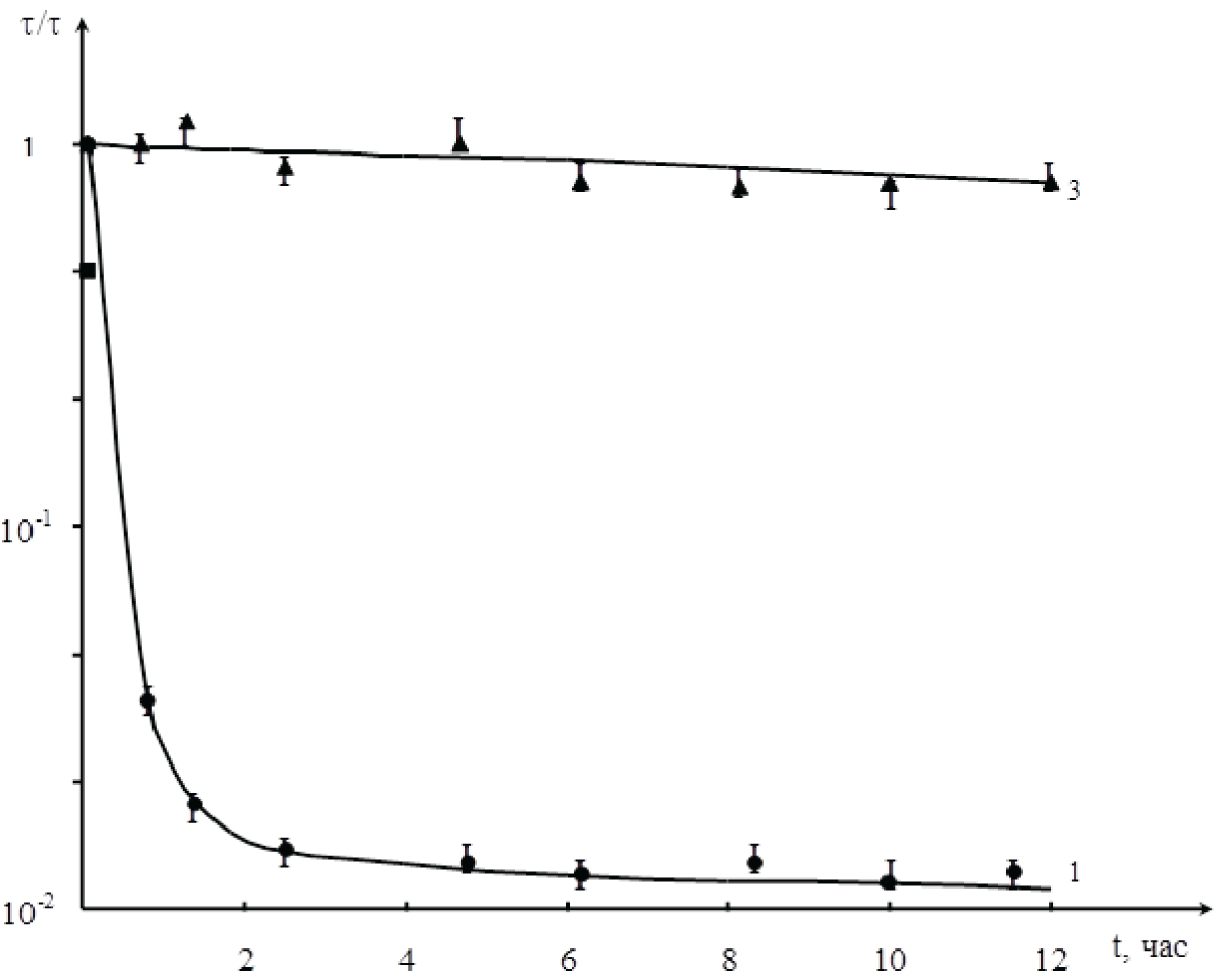
In order to evaluate whether the clusters of atoms of gadolinium might be used for designing efficient semiconductor devices, it is necessary to find out how they influence the lifetime of minority charge carriers. Such studies are also of interest for revealing the state of clusters of atoms of gadolinium in silicon matrix, and their interaction with other impurity atoms and defects. Therefore, to study the lifetime of minority charge carriers, we chose silicon doped with gadolinium with a concentration of NGd≈1017 cm-3. After each stage of annealing, the samples were subjected to treatment in a polishing etchant under identical conditions, which made it possible to remove oxide layers and other defects from the surface that occur during heat treatment.
Figure 10 shows the dependences of a lifetime of minority charge carriers on annealing time at T=1000°C for Si<P, Gd> samples and reference samples.
Figure 10: Dependence of lifetime of minority charge carriers on the duration of thermal annealing, Т=1000 0С. 1-Si; 2-Si<P,Gd>.
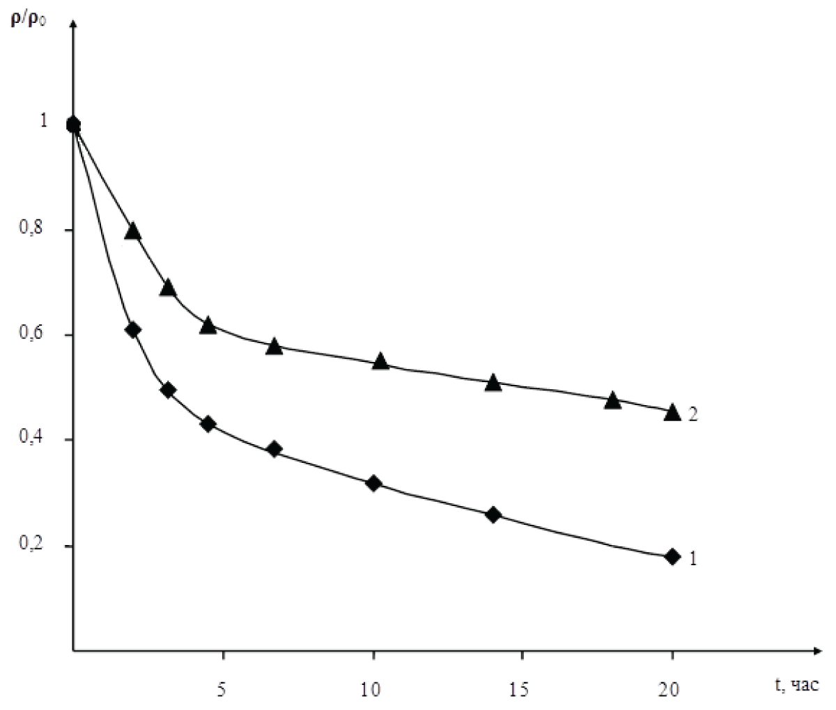
Figure 11 shows the relative change in the resistivity of Si<P, Gd> (NGd≈1017 cm-3) as a function of the time of additional thermal annealing at T = 500 0С.
Figure 11: Relative change in the resistivity of the material as a function of duration of additional thermal annealing at T = 500 0C. Samples: 1- original Si; 2-Si<P,Gd> (NGd =1017 см-3).
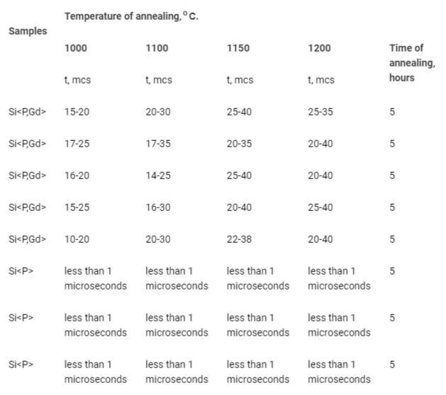
Table 1 lists the values of τ for samples depending on the annealing temperature. In this case, the annealing time is 5 hours.
Table 1: Dependence of the lifetime of minority charge carriers on the annealing temperature.
As can be seen from Table 1, in the Si<P,Gd> samples, the lifetime of minority charge carriers in a wide temperature range is quite stable. It should be noted that in the Si<P,Gd> samples, the authors had observed an even increase in τ compared to initial values. These results show that the presence of impurity gadolinium atoms almost completely suppresses the generation of recombination centers, which always exist and are generated in single crystals during heat treatment.
As can be seen from Figure 6, the lifetime of minority charge carriers for all types of materials before heat treatment was approximately the same order of magnitude (16 - 32 μs), the lifetime of minority charge carriers in reference samples decreases sharply as a function of heat treatment for 1 ÷ 1.5 hours almost to several µseconds. At the end of the heat treatment, τ becomes less than one microsecond. At the same time, the lifetime of minority charge carriers in Si<P,Gd> samples practically remains constant at all heat treatment times.
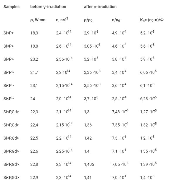
It was also found that Si<P,Gd> samples are characterized by increased radiation resistance. Table 2 shows the change in the electrical parameters of the Si<P,Gd> samples before and after γ-irradiation with a dose of 109 R.
Table 2: Changes in the electrical parameters of Si<P,Gd> samples under γ-irradiation.
Thus, one can conclude that in silicon doped with gadolinium, the lifetime of minority charge carriers manifests comparative stability during additional thermal annealing. It’s worthwhile noting that the increased radiation resistance during γ-irradiation is also manifested in this case.
The positive effect of additional doping with gadolinium consists in the fact that any thermal annealing, which causes the generation of thermal donors and undesirable activation of impurity atoms, leads clusters of gadolinium atoms to remove the stress field and bring the system to an equilibrium state, i.e., to increase the entropy of the system. This can be confirmed by the results of additional experiments carried out in our laboratory on an infrared microscopic study of the distribution of gadolinium atoms in gadolinium-doped silicon.
It was found that during heat treatment in Si<P,Gd> samples, gadolinium atoms are clearly deposited around stress fields, forming clusters of impurity atoms of gadolinium. Therefore, the stability of the parameters of Si (ρ and τ) doped with gadolinium during heat treatment is explained by the active capture of defects and impurity atoms by clusters of gadolinium atoms.
A technology of step-by-step low-temperature diffusion doping of gadolinium into silicon has been developed that allows the clusters of impurity atoms of gadolinium to be uniformly distributed throughout the entire bulk of a material. The presence of such clusters makes it possible not only to control the properties of semiconductor material but also allow to the use of such materials in the development of novel designs of semiconductor devices. It was shown that, unlike the samples obtained under the high-temperature diffusion doping technique, in the samples obtained under the novel technology the team had not detected any surface erosion or formation of alloys and silicide in the near-surface region. It has been revealed that in the case of a step-by-step low-temperature diffusion, the temperature and diffusion time affect not only the impurity penetration depth but also the size of the clusters being formed.
A comprehensive study of the physical properties of the silicon-containing ordered clusters of impurity atoms of gadolinium and scandium may contribute to the discovery of novel physical phenomena that have not previously been found in doped semiconductor materials and in semiconductors with nanostructures alike. Controlling the state and distribution of clusters of impurity atoms of gadolinium and scandium in the silicon matrix makes it possible to create a new class of semiconductor materials with unique functionality, as well as to create on its basis a new class of devices for optoelectronics and microelectronics.
The experimental data shows that the atoms of gadolinium and scandium that are located in interstitial unstable states in the lattice, in the process of low-temperature doping tend to migrate to a more energetically favorable (quasi-equilibrium state) i.e., interact to form a cluster. In this case, single gadolinium atoms leave the matrix, and the system passes into the most energetically favorable state. The process of formation and interaction of clusters, due to gadolinium atoms, significantly removes the deformation stress in the crystal. In this case, both oxygen atoms and other lattice defects tend to be the main stimulators of the trend; accordingly, the formation of clusters of gadolinium impurity atoms has a strong gettering effect, which significantly reduces the concentration of uncontrolled impurities contaminating the crystal and suppresses the formation of thermal donors.
It has been established that Si<P,Gd> samples have increased thermal and radiation resistance. Silicon doped with gadolinium significantly stabilizes the lifetime of minority charge carriers during additional thermal annealing, and is also characterized by increased radiation resistance under γ-irradiation. Thus, clusters of impurity atoms of gadolinium most probably lead to a strong gettering effect.
An analysis of the experimental results shows that the diffusion coefficients and activation energies of scandium impurities in silicon are in the range of values characteristic of the diffusion of typical elements belonging to group III, as well as for other rare earth elements that appear to be substitutional impurities and diffuse via the crystal lattice sites. It could be suggested that the scandium atoms belonging to the same group could also represent substitutional impurities and diffuse, like other rare earth elements, through the sites of the silicon crystal lattice. An analysis of the experimental results related to the process of formation of clusters of impurity atoms of gadolinium and scandium also proved that it is possible to relocate the resulting clusters to the desired place.
A comparative analysis of the experimental data with early experimental results related to the diffusion of rear earth elements into silicon that were taken using radioactive and other methods had shown that the method of applying a dopant and the diffusion atmosphere does not significantly affect the diffusion parameters of rear earth elements in silicon. Thus, it can be assumed that rare-earth impurities of scandium (III group), tend to behave also as substitutional impurities and diffuse over the crystal lattice sites (vacancy diffusion mechanism) of silicon.
Egamberdiev BE. Electron spectroscopic studies of the physical properties of epitaxial combinations and ion-implanted layers in silicon. Doctoral dissertation. 2003; С 243.
Egamberdiev BE, Abdugabborov M. Study of some features of the distribution profiles of implanted Mn, Fe and Ni atoms in Si. Vestnik TSTU. 1994; Т.1-2: С.39-44.
Egamberdiev BE, Iliev KhM, Nasriddinov SS, Toshev AR, Zoirova ME. Photoelectric properties of silicon-based solar cells implanted with rare earth elements. Conference. Russia. Vladivostok. 2006; 204-208.
Egamberdiev BE. Mallaev AS. Silicon silicide structures based on ion doping. T.:ed. "Science and Technology". 2019; 168с.
Egamberdiev BE, Rakhmanov AT. Study by the ROP method of the distribution profile of ion-implanted iron atoms in silicon.Science and world. 2018;1:1(53);с.57-60.
Egamberdiev BE, Rakhmanov AT, Mallaev AS, Rozikov S. Research by method of Rutherford backscannering distribution of ion-implanted atoms of Fe in Si. Science and world. 2018; 1(53):1; 57-60.
Miquita DR, Paniago R, Rodrigues WN, Moreira MV, Pfannes H-D, Oliveira AG. Growth of (3-FeSi2 layers on Si(lll) by solid phase and reactive deposition epitaxies. Thin Solid Films. 2005;493:30-34.
Egamberdiev BE, Mallaev AS, Toshev AR. Features of the electronic structure of ion-implanted Ni, Fe, and Co layers in silicon. Mezhdunarodnaya konferenciya. Rossiya [International Conference], Russian, Tomsk. 2009;77-80.
Suzdalev IP. Nanotechnology: physico-chemistry of nanoclusters, nanostructures and nanomaterials. M.Com Book. 2006; 592.
Bagraev NG, Romanov VV. Magnetism of AIIIBV crystals doped with rare elements. FTP. 2005;39(10):1173-1182.
Abdurakhmanov BA, Egamberdiev BE, Iliev KhM, Tachilin SA, Toshev AR. The influence of silicon-germanium microheterojunctions on the parameters of silicon solar cells. J Electron Mater Process. Moldova. 2010;(5):124-126.
Gavrilov G, Krivchitch A, Lebedev V. Application of nuclear reaction. Analysis for aging investigations of detectors. Nucl Instr Meth A. 2003;515:108-117.
Egamberdiev BE, Iliev KhM, Tachilin SA, Toshev AR. Radiation stability of silicon solar cells doped with holmium. XI International Conference "Solid State Physics". Ust-Kamenogorsk, Kazakhstan. June 9-12, 2010.
Daliev KhS, Dekhkanov MSh, Erugliev UK, Norkulov ShB, Ergashev ZhA. Capacitive spectroscopy of defects in silicon doped with gadolinium atoms. Phys Semicond Microelectron. 2019;1(01):15-17.
Zhuravel LV, Latukhina NV, Blytushkina EYu. The influence of doping with rare earth elements on the structure of the surface layer of silicon. Izv Univ Mater Electron Technol. 2004;(3):72-74.
Latukhina NV, Volkov AV, Zhuravel LV, Lebedev VM. The role of microdeformations during pore formation in silicon doped with rare earth elements. Proc Third Int Sci-Tech Conf "Metalphysics, Mechanics of Materials, Nanostructures and Deformation Processes" Metaldeform-2009. Samara. 2009;1:30-34.
Lebedev VM, Lukyanov YG, Smolin VA. Analytical complex for studying materials using nuclear microanalysis methods. Tr XIII Int Conf Electrostatic Accelerators. Obninsk (Russia). 2001:60-66.
Latukhina NV, Lebedev VM. Distribution of components in the structures silicon - silicon oxide and silicon - oxide of a rare earth element. Lett Tech Phys. 2005;31(13):58-64.
Aleksandrov OV, Zakhain AO, Sobolev NA. Electrophysical properties of silicon layers implanted with erbium and oxygen ions in a wide range of doses and heat-treated in different temperature conditions. FTP. 2002;36(3):379-382.
Latukhina NV, Volkov AV, Zhuravel LV, Lebedev VM. The role of microdeformations during pore formation in silicon doped with rare earth elements. Proc Third Int Sci-Tech Conf "Metalphysics, Mechanics of Materials, Nanostructures and Deformation Processes" Metaldeform-2009. Samara. 2009;1:30-34.
Zhuravel LV. Effect of doping with rare earth elements on the structure of the surface layer of silicon. Izv Univ Mater Electron Technol. 2004;(3):72-74.
Fistul VI. Atoms of dopant impurities in semiconductors. Moscow: Fizmatlit; 2004; 432.
BE E, S DA, Kh KH, B NO, UK E. On how Doping with Atoms of Gadolinium and Scandium affects the Surface Structure of Silicon. IgMin Res. Jun 26, 2024; 2(6): 476-483. IgMin ID: igmin206; DOI:10.61927/igmin206; Available at: igmin.link/p206
Address Correspondence: Egamberdiev BE, National University -affiliated Research Institute of Semiconductor Physics and Microelectronics, Tashkent, 100057, Republic of Uzbekistan, Email: [email protected]; [email protected]
How to cite this article: BE E, S DA, Kh KH, B NO, UK E. On how Doping with Atoms of Gadolinium and Scandium affects the Surface Structure of Silicon. IgMin Res. Jun 26, 2024; 2(6): 476-483. IgMin ID: igmin206; DOI:10.61927/igmin206; Available at: igmin.link/p206
Figure 2: Concentration profiles of Gd in silicon samples no...
Figure 3: Concentration profiles of Gd in silicon samples su...
Figure 4: Concentration profiles of Sc in silicon samples su...
Figure 5: Concentration profiles of Gd in silicon diffusion ...
Figure 6: Micrograph of the bulk of a silicon sample into wh...
Figure 7: Micrograph of a silicon sample doped with gadolini...
Figure 8: Micrograph of a silicon sample obtained by two-sta...
Figure 9: Micrograph of a silicon sample obtained by three-s...
Figure 10: Dependence of lifetime of minority charge carriers...
Figure 11: Relative change in the resistivity of the material...
Table 1: Dependence of the lifetime of minority charge carr...
Table 2: Changes in the electrical parameters of Si<P,Gd...
Egamberdiev BE. Electron spectroscopic studies of the physical properties of epitaxial combinations and ion-implanted layers in silicon. Doctoral dissertation. 2003; С 243.
Egamberdiev BE, Abdugabborov M. Study of some features of the distribution profiles of implanted Mn, Fe and Ni atoms in Si. Vestnik TSTU. 1994; Т.1-2: С.39-44.
Egamberdiev BE, Iliev KhM, Nasriddinov SS, Toshev AR, Zoirova ME. Photoelectric properties of silicon-based solar cells implanted with rare earth elements. Conference. Russia. Vladivostok. 2006; 204-208.
Egamberdiev BE. Mallaev AS. Silicon silicide structures based on ion doping. T.:ed. "Science and Technology". 2019; 168с.
Egamberdiev BE, Rakhmanov AT. Study by the ROP method of the distribution profile of ion-implanted iron atoms in silicon.Science and world. 2018;1:1(53);с.57-60.
Egamberdiev BE, Rakhmanov AT, Mallaev AS, Rozikov S. Research by method of Rutherford backscannering distribution of ion-implanted atoms of Fe in Si. Science and world. 2018; 1(53):1; 57-60.
Miquita DR, Paniago R, Rodrigues WN, Moreira MV, Pfannes H-D, Oliveira AG. Growth of (3-FeSi2 layers on Si(lll) by solid phase and reactive deposition epitaxies. Thin Solid Films. 2005;493:30-34.
Egamberdiev BE, Mallaev AS, Toshev AR. Features of the electronic structure of ion-implanted Ni, Fe, and Co layers in silicon. Mezhdunarodnaya konferenciya. Rossiya [International Conference], Russian, Tomsk. 2009;77-80.
Suzdalev IP. Nanotechnology: physico-chemistry of nanoclusters, nanostructures and nanomaterials. M.Com Book. 2006; 592.
Bagraev NG, Romanov VV. Magnetism of AIIIBV crystals doped with rare elements. FTP. 2005;39(10):1173-1182.
Abdurakhmanov BA, Egamberdiev BE, Iliev KhM, Tachilin SA, Toshev AR. The influence of silicon-germanium microheterojunctions on the parameters of silicon solar cells. J Electron Mater Process. Moldova. 2010;(5):124-126.
Gavrilov G, Krivchitch A, Lebedev V. Application of nuclear reaction. Analysis for aging investigations of detectors. Nucl Instr Meth A. 2003;515:108-117.
Egamberdiev BE, Iliev KhM, Tachilin SA, Toshev AR. Radiation stability of silicon solar cells doped with holmium. XI International Conference "Solid State Physics". Ust-Kamenogorsk, Kazakhstan. June 9-12, 2010.
Daliev KhS, Dekhkanov MSh, Erugliev UK, Norkulov ShB, Ergashev ZhA. Capacitive spectroscopy of defects in silicon doped with gadolinium atoms. Phys Semicond Microelectron. 2019;1(01):15-17.
Zhuravel LV, Latukhina NV, Blytushkina EYu. The influence of doping with rare earth elements on the structure of the surface layer of silicon. Izv Univ Mater Electron Technol. 2004;(3):72-74.
Latukhina NV, Volkov AV, Zhuravel LV, Lebedev VM. The role of microdeformations during pore formation in silicon doped with rare earth elements. Proc Third Int Sci-Tech Conf "Metalphysics, Mechanics of Materials, Nanostructures and Deformation Processes" Metaldeform-2009. Samara. 2009;1:30-34.
Lebedev VM, Lukyanov YG, Smolin VA. Analytical complex for studying materials using nuclear microanalysis methods. Tr XIII Int Conf Electrostatic Accelerators. Obninsk (Russia). 2001:60-66.
Latukhina NV, Lebedev VM. Distribution of components in the structures silicon - silicon oxide and silicon - oxide of a rare earth element. Lett Tech Phys. 2005;31(13):58-64.
Aleksandrov OV, Zakhain AO, Sobolev NA. Electrophysical properties of silicon layers implanted with erbium and oxygen ions in a wide range of doses and heat-treated in different temperature conditions. FTP. 2002;36(3):379-382.
Latukhina NV, Volkov AV, Zhuravel LV, Lebedev VM. The role of microdeformations during pore formation in silicon doped with rare earth elements. Proc Third Int Sci-Tech Conf "Metalphysics, Mechanics of Materials, Nanostructures and Deformation Processes" Metaldeform-2009. Samara. 2009;1:30-34.
Zhuravel LV. Effect of doping with rare earth elements on the structure of the surface layer of silicon. Izv Univ Mater Electron Technol. 2004;(3):72-74.
Fistul VI. Atoms of dopant impurities in semiconductors. Moscow: Fizmatlit; 2004; 432.


 スキャンしてリンクを取得