Welcome to IgMin Research – an Open Access journal uniting Biology, Medicine, and Engineering. We’re dedicated to advancing global knowledge and fostering collaboration across scientific fields.
At IgMin Research, we bridge the frontiers of Biology, Medicine, and Engineering to foster interdisciplinary innovation. Our expanded scope now embraces a wide spectrum of scientific disciplines, empowering global researchers to explore, contribute, and collaborate through open access.
Welcome to IgMin, a leading platform dedicated to enhancing knowledge dissemination and professional growth across multiple fields of science, technology, and the humanities. We believe in the power of open access, collaboration, and innovation. Our goal is to provide individuals and organizations with the tools they need to succeed in the global knowledge economy.
IgMin Publications Inc., Suite 102, West Hartford, CT - 06110, USA
In single colloidal nanocrystals of narrow-gap semiconductors PbS and InSb, current instability in the form of quasi-periodic spikes and current resonance peaks was studied by measuring on a scanning probe microscope and analyzing Current-Voltage Characteristics (CVC). The observed phenomena are explained in models of the wave de Broglie process and Bloch oscillations. Statistically, the percentages of such samples and the parameters of oscillations on the current-voltage characteristic are higher, the larger the size quantization parameter, determined by the de Broglie wavelength. A possible practical use is the generation and recording of terahertz radiation modulated by ultrashort pulses.
Research into charge instability and current oscillations in semiconductor crystals is an important area of science and technology. In recent years, there has been increased interest in theoretical studies of a quantum mechanical phenomenon in crystals - Bloch oscillations, including in connection with studies of low-dimensional semiconductor structures: Bloch vibrational resonance in materials with high conductivity [11Singh S, Battiato M. Effect of Strong Electric Fields on Material Responses: The Bloch Oscillation Resonance in High Field Conductivities. Materials. 2020; 13(5):1070. DOI:10.3390/ma13051070.]; a new type of Bloch oscillations, the periodicity of which is an integer [22Höller J, Alexandradinata A. Topological Bloch oscillations. Phys Rev B. 2018; 98(2):024310. DOI:10.1103/PhysRevB.98.024310.]; theory of spontaneous terahertz radiation of a Bloch electron crossing one energy miniband of a superlattice [33Sokolov VN, Iafrate GJ. Spontaneous emission of Bloch oscillation radiation under the competing influences of microcavity enhancement and inhomogeneous interface degradation. J Appl Phys. 2014; 115:054307. DOI:10.1063/1.4863599.]; anharmonic Bloch oscillations in electrically biased superlattices [44Ivanov KA, Girshova EI, Kaliteevsky MA, Clark SJ, Gallant AJ. Anharmonic Bloch oscillations of electrons in electrically biased superlattices. Semiconductors. 2016; 50(11):1484. DOI:10.21883/ftp.2016.11.43778.10.]; study of the behavior of Bloch oscillations in AlGaAs/GaAs superlattices using the Monte Carlo method [55Moravcova H, Voves J. Physica E. Bloch oscillations in superlattices: Monte-Carlo analysis using 2D scattering model. Low-dimensional Systems and Nanostructures. 2003; 17:307. DOI:10.1016/S1386-9477(02)00818-4.]; theoretical study of the scattering of oscillating electrons in a superlattice of quantum dots, which can be strongly suppressed by a suitable choice of the magnitude and direction of the field, and calculations under the assumption that in an isolated zero-dimensional quantum dot, there is only one quantization level [66Dmitriev IA, Suris RA. Electron localization and bloch oscillations in quantum-dot superlattices under a constant electric field. Semiconductors. 2001; 35(2):219.]. The predicted practical application of the phenomenon is the generation and recording of terahertz radiation modulated by supershort pulses [33Sokolov VN, Iafrate GJ. Spontaneous emission of Bloch oscillation radiation under the competing influences of microcavity enhancement and inhomogeneous interface degradation. J Appl Phys. 2014; 115:054307. DOI:10.1063/1.4863599.].
All of these reference articles note that the experimental observation of Bloch oscillations in ordinary (large) single crystals, unlike, for example, superlattices, is practically impossible due to the scattering influence of structural defects and thermal vibrations of the lattice (phonons). However, it should be noted that their observation in two-dimensional superlattices, in which these influences can actually be eliminated, is difficult due to the weakening of the effect due to imperfections of the structure [66Dmitriev IA, Suris RA. Electron localization and bloch oscillations in quantum-dot superlattices under a constant electric field. Semiconductors. 2001; 35(2):219.]. Therefore, the experimental observation of oscillations obtained in [77Sapienza R, Toninelli C, Otonc CJ. Bloch oscillations and resonant Zener tunneling of light in optical superlattices. Proc SPIE. 2005;2:421. DOI:10.1117/12.608205.,88Geiger ZA, Fujiwara KM, Singh K. Observation and Uses of Position-Space Bloch Oscillations in an Ultracold Gas. Phys Rev Lett. 2018;120:213201. DOI:10.1103/PhysRevLett.120.213201.] is defined by the authors as a great scientific achievement.
The quantum manifestation of Bloch oscillations is associated with electronic conductivity in the crystal. In a quantum dot, as a quasi-zero-dimensional formation, the conductivity is determined by the recharging of the nanocapacitor and the ballistic jump of the electron, which was first studied theoretically and experimentally by Ekimov A.I. with collaborators [99Ekimov AI, Onushchenko AA. Quantization of the energy spectrum of holes in the adiabatic potential of the electron. Lett J Theor Exp Phys. 1984; 40(8):337.]. At the same time, specific manifestations were discovered - the Coulomb blockade and Coulomb “ladder”. This model is often used in theoretical calculations and evaluations of reduced-dimensional structures.
A quantum-sized particle, in fact, is not a zero-dimensional formation, having the properties of an extended potential well. Its conductivity is more complex, determined by several physical processes [1010Zhukov ND, Gavrikov MV. Tech Phys Lett. 2022; 48(8):18. DOI:0.21883/PJTF.2022.08.52361.19090.]. In a perfect nanocrystal with dimensions of more than several values of the lattice constant, the conditions for the applicability of physical models of a large crystal are met. Theoretically, these issues are discussed in detail in a number of publications and monographs, for example [1111Dragunov VP, Unknown IG, Gridchin VA. The Influence of Different Type Irradiations on the Surface States Parameters of Si-SiO2 Structures. Fundamentals of Nanoelectronics. Moscow: Logos; 2006. p. 495.,1212Martinez B, Livache C, Notemgnou LDM. Synthesis and properties of mercury selenide colloidal quantum dots. ACS Appl Mater Interfaces. 2017; 9(41):36173.], where the processes are described by solutions of the Schrödinger equation for different versions, taking into account electron tunneling through barriers at the boundaries and its reflections from them. In [1313Lesovik GB, Sadovsky IA. Scattering matrix approach to the description of quantum electron transport. Adv Phys Sci. 2011; 181(10):1041. DOI:10.3367/UFNr.0181.201110b.1041.], the theory of quantum electron transport in meso- and nanoconductors was developed using the method of scattering matrices, an alternative to the more usual approach using kinetic equations or Green’s functions. In [1414Glinsky GF. A simple numerical method for determining the energy spectrum of charge carriers in semiconductor heterostructures. Tech Phys Lett. 2018; 44(6):17. DOI:10.21883/PJTF.2018.06.45763.17113.], the process of electron transport in a semiconductor nanostructure is considered a quantum wave process with the inherent nature of quantum resonance. A number of works have investigated issues of electronic states, including under transport conditions, in arrays of quantum dots [1515Райх КВ. Adv Phys Sci. 2020; 190(10):1063.-1717Zhu J, Hersam MC. Assembly and Electronic Applications of Colloidal Nanomaterials. Adv Mater. 2017; 29:1603895.].
Experimental studies of electron transport in individual nanoparticles are extremely rare. In [1818Diaconescu B, Padilha LA, Nagpal P, Swartzentruber BS, Klimov VI. Measurement of electronic states of PbS nanocrystal quantum dots using scanning tunneling spectroscopy: the role of parity selection rules in optical absorption. Phys Rev Lett. 2013; 110:127406. DOI:10.1103/PhysRevLett.110.127406.], such a study was carried out on individual quantum dots of PbS nanocrystals using scanning probe microscopy using one or two monolayer films of nanocrystals. We have carried out systematic studies of electron transport in nanoparticles of CdSe, PbS, InSb, and HgSe according to the measurement scheme [1818Diaconescu B, Padilha LA, Nagpal P, Swartzentruber BS, Klimov VI. Measurement of electronic states of PbS nanocrystal quantum dots using scanning tunneling spectroscopy: the role of parity selection rules in optical absorption. Phys Rev Lett. 2013; 110:127406. DOI:10.1103/PhysRevLett.110.127406.], as reported in a number of works [1010Zhukov ND, Gavrikov MV. Tech Phys Lett. 2022; 48(8):18. DOI:0.21883/PJTF.2022.08.52361.19090.,1919Gavrikov MV, Glukhovskoy EG, Zhukov ND. Quantum conductivity in single and coupled quantum-sized particles of narrow-gap semiconductors. Semiconductors. 2023; 57(5):338. DOI:10.21883/FTP.2023.05.56200.27k.], including two to seven monolayer structures formed by the Langmuir-Blodgett film method [1919Gavrikov MV, Glukhovskoy EG, Zhukov ND. Quantum conductivity in single and coupled quantum-sized particles of narrow-gap semiconductors. Semiconductors. 2023; 57(5):338. DOI:10.21883/FTP.2023.05.56200.27k.]. At the same time, in addition to quasi-periodic low-current oscillations, we observe sharp (resonant) current peaks, which we explain in the model of the de Broglie wave process of electron transport and call the phenomenon quantum conductivity.
In this work, we continued the study of single colloidal nanocrystals of narrow-gap semiconductors with the highest size quantization parameters - indium antimonide (NC-InSb) and lead sulfide (NC-PbS). For analytical modeling, we used comparisons of properties with variants of relatively wide-gap cadmium selenide (NC-CdSe) and gapless mercury selenide (NC-HgSe). Technological properties and features of manufacturing nanoparticles of all variants can be found in our works [2020Zhukov ND, Smirnova TD, Khazanov AA, Tsvetkova OYu, Shtykov SN. Properties of semiconductor colloidal quantum dots obtained under controlled synthesis conditions. Semiconductors. 2021; 55(12):1203. DOI:10.21883/FTP.2021.12.51706.9704.-2222Krylsky DV, Zhukov ND. Synthesis, composition, photoluminescence, and stability of properties of colloidal InSb-based quantum dots. Tech Phys Lett. 2019; 45(16):10. DOI:10.21883/PJTF.2019.16.48147.17665.].
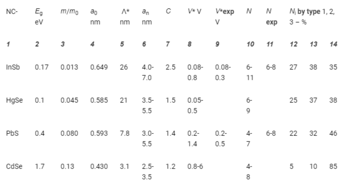
Selected data are given in Table 1. The semiconductor parameters used – band gap Eg, the ratio of effective electron mass m to free electron mass m0, lattice constant a0 – were obtained from the Internet reference book [2323Chemical encyclopedia. http://xumuk.ru/encyklopedia].
Table 1: Semiconductor parameters and experimental data for nanocrystals.
The technological process of synthesis of nanoparticles, at its core, is as follows. A solution with a metal precursor is placed in a 50 ml three-neck flask. At a selected temperature, the preparatory process is carried out with intensive stirring for a selected time in an atmosphere of dried nitrogen. Then the temperature is reduced to the synthesis temperature and a selected amount of non-metal precursor solution is quickly introduced into the flask. Next, the synthesis is carried out for a variable time, after which the reaction is stopped by placing the flask in a special refrigerator. The resulting darkish solution is then uncorked in air and the nanoparticles are precipitated by adding ethanol and centrifugation. The mother liquor is drained, and the precipitate is dispersed in toluene. The cleaning procedure is repeated. To do this, the solution in pure toluene is first centrifuged without adding ethanol to get rid of the lamellar phase formed as a result of the complexation of the metal with the solvent. In this case, only the stable solution is retained and the gray precipitate is discarded. A limited amount of ethanol is then added and centrifuged. The resulting fractions are stored in a clean, inert environment until used.
Each batch of samples was monitored on a random selection of nanoparticles using Scanning Electron Microscopy (SEM) for stoichiometric composition and Transmission Electron Microscopy (TEM) for shape and size. Direct measurements of the sizes of nanoparticles in a colloidal solution were carried out using a Zetasizer Nano ZS laser analyzer (Malvern Panalytical Ltd., United Kingdom) using a glass cuvette.
Experiments were carried out on random samples of a large number (more than 200) samples of nanocrystals by TEM control of their shape and size on a Libra-120 transmission electron microscope (CarlZeiss, Germany) and measurements of current-voltage characteristics (CVC) of single nanocrystals in a sealed compact chamber scanning probe microscope (SPM).
Measurements of current-voltage characteristics (CV characteristics) were carried out on a SOLVERNano scanning probe microscope under sealed chamber conditions, in field emission modes from the probe at relatively large probe-sample nanogap values (~ 5 nm) and “minus” polarity on the probe. The conditions for such use of a tunnel microscope were studied and substantiated in our work [2424Zhukov ND, Gavrikov MV. Int Scientific Res J. 2021; 8(110):19. DOI:https://doi.org/10.23670/IRJ.2021.110.8.004.].
In a quantum-sized nanocrystal, we consider conductivity in the model of a one-dimensional deep extended quantum well with manifestations of electron injection, its transport, and tunnel emission in it. The motion of an electron inside a nanocrystal is described by the solution of the Schrödinger equation and the de Broglie wave process. The consideration is based on a model of one-dimensional single-electron motion. The electron energy values Ẽqn are determined by the resonance of the electron wave process and are calculated depending on the type of semiconductor (m/m0 values) and the dimensions of the nanocrystal an. Formulas for the total energy Ẽqn, de Broglie wavelength Λ for an electron and the probability K* of an electron passing through a nanocrystal as a deep rectangular extended potential well in a one-dimensional one-electron model can be obtained in the following form [1111Dragunov VP, Unknown IG, Gridchin VA. The Influence of Different Type Irradiations on the Surface States Parameters of Si-SiO2 Structures. Fundamentals of Nanoelectronics. Moscow: Logos; 2006. p. 495.]:
Ẽqn= h2q2(8man2)-1 ≈ 0.37q2(m/m0)-1an-2; (1)
Λ = h(2mẼk)-1/2 ≈ 1.2(Ẽkm/m0)-1/2 = 2an/ V*; (2)
K* ∝ exp[4πan(2mẼk)1/2/h4πan(2mẼk)1/2/hIvanov KA, Girshova EI, Kaliteevsky MA, Clark SJ, Gallant AJ. Anharmonic Bloch oscillations of electrons in electrically biased superlattices. Semiconductors. 2016; 50(11):1484. DOI:10.21883/ftp.2016.11.43778.10.] ≈ exp[-4(q2-2.7Van2m/m0)1/2] = exp[4V *4V *Ivanov KA, Girshova EI, Kaliteevsky MA, Clark SJ, Gallant AJ. Anharmonic Bloch oscillations of electrons in electrically biased superlattices. Semiconductors. 2016; 50(11):1484. DOI:10.21883/ftp.2016.11.43778.10.] (3)
where: Ẽk~(Ẽqn-V) – kinetic energy of the electron; V*~(q2-2.7Van2m/m0)1/2 – dimensionless parameter depending on the voltage V – potential difference on the nanocrystal; for calculations: Ẽk, Ẽqn, V– in electronvolts, Λ and an – in nanometers. Formula (3) is obtained as the probability of an electron passing through an extended rectangular potential barrier of width an.
The formula for the Current-Voltage Characteristic (CVC) for the case when the current is limited by the probability of an electron passing through a nanocrystal as an extended potential barrier can be written, based on formula (3), in the following form:
I ∝ K* ∝ exp[4V*4V*Ivanov KA, Girshova EI, Kaliteevsky MA, Clark SJ, Gallant AJ. Anharmonic Bloch oscillations of electrons in electrically biased superlattices. Semiconductors. 2016; 50(11):1484. DOI:10.21883/ftp.2016.11.43778.10.] (4)
The quantum-size effect on electronic conductivity depends on the ratio an and Λ~2an/V*. For the confinement condition, (Λ/an)>1, it is necessary that the following relation be satisfied: 0≤V*<2. In this case, Λ can be taken as a size quantization parameter for a semiconductor. Table 1 presents the values of this parameter Λ*, calculated (conditionally) for Ẽk ~ Eg/2.
The condition for resonance and quantum conductivity G can be assessed by differentiating the current-voltage characteristic of formula (4):
G = dI/dV = -4I(dV*/dV) ≈ 5.4(I/V*)an2m/m0 (5)
As follows from formula (5), the condition for resonance (and quantum conductivity) will be V*~0, that is, q2~2.7Van2m/m0. Physically, this condition means that the potential barrier becomes transparent [1111Dragunov VP, Unknown IG, Gridchin VA. The Influence of Different Type Irradiations on the Surface States Parameters of Si-SiO2 Structures. Fundamentals of Nanoelectronics. Moscow: Logos; 2006. p. 495.].
Bloch oscillations are a quantum mechanical phenomenon in solid-state physics, which is caused by the spatiotemporal instability of a quantum particle (electron) located in the periodic potential of a crystal lattice under the influence of an electric field. The physical essence of the phenomenon lies in the fact that, under the influence of an external constant field in a crystal, an electron in the space of the band diagram E(k) undergoes oscillatory motion along the kx axis near the origin of coordinates in a pattern of repeating Brillouin zones on a limited segment of the component axis.
A more detailed description of research methods can be obtained from our works [1010Zhukov ND, Gavrikov MV. Tech Phys Lett. 2022; 48(8):18. DOI:0.21883/PJTF.2022.08.52361.19090.,1919Gavrikov MV, Glukhovskoy EG, Zhukov ND. Quantum conductivity in single and coupled quantum-sized particles of narrow-gap semiconductors. Semiconductors. 2023; 57(5):338. DOI:10.21883/FTP.2023.05.56200.27k.,2525Zhukov ND, Gavrikov MV, Shtykov SN. Electron-photon interactions in the conditions of dimensional conductivity restrictions in semiconductor single quantum-size particles in interelectrodic nanogapSemiconductors. 2022; 56(6):552. DOI:10.21883/FTP.2022.06.52588.9809.].
Experimental measurements of the current-voltage characteristics were carried out on all studied variants in quantities, for each of them, of 80 - 90 nanocrystals in external voltage modes of up to 4 V and current of up to 150 nA. The proportion of the number of Ni samples with current-voltage characteristics with pronounced features is from 15 to 65%, depending on the type of semiconductor and the size of the nanocrystals (Table 1, columns 12 and 13). Moreover, the higher the size quantization parameter Λ*, the higher it is (Table 1, Article 5).
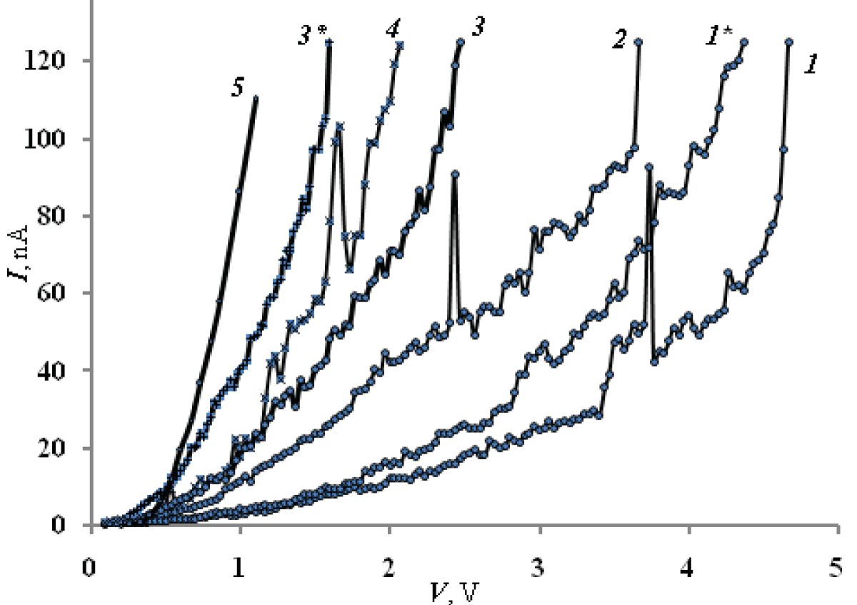
Depending on the type of semiconductor (m/m0) and the size an of the nanocrystals, three types of curves appear on the experimental current-voltage characteristics (Figure 1): 1 (curves 3*, 5) – completely or almost without features; 2 (cr. 1*, 3) – with features such as quasiperiodic low-current pulsations; 3 (cr. 1, 2, 4) – with features of type 2 and sharp large single (one or two) current peaks. We explain the differences in the types of current-voltage characteristics by the degree of manifestation of size quantization: curves of type 1 - its absence, 2 - weak, 3 - strong. The degree of quantum-size manifestations for different cases can be estimated by the parameter C~(m/m0)-1an-2. Table 1 (Article 7) shows the values of parameter C calculated for the maximum of the distribution curve an.
Figure 1: Current-voltage characteristics for different variants of nanocrystals: 1, 1* – NC-InSb; 2 – NC-HgSe; 4 – NC-PbS; 3, 3*– NC-CdSe; 5 – micro-InSb.
Type 1 current-voltage characteristics in their different sections were approximated by exponentials Iet~exp(αV) and It~exp(-β/V) with parameters α~10 and β~2, which corresponds to the tunnel-emission model [1010Zhukov ND, Gavrikov MV. Tech Phys Lett. 2022; 48(8):18. DOI:0.21883/PJTF.2022.08.52361.19090.,2525Zhukov ND, Gavrikov MV, Shtykov SN. Electron-photon interactions in the conditions of dimensional conductivity restrictions in semiconductor single quantum-size particles in interelectrodic nanogapSemiconductors. 2022; 56(6):552. DOI:10.21883/FTP.2022.06.52588.9809.]. Type 3 current-voltage characteristics were practically not observed for NC-CdSe but dominated for NC-PbS, NC-HgSe, and especially, NC-InSb. In this case, the current-voltage characteristics, on average, were well approximated by the dependence IQP~Vγ with the parameter γ~2 for NC-CdSe and γ~3 for NC-PbS, NC-InSb and NC-HgSe. This power-law dependence (with a coefficient of two to three) is explained by the model of current limitation by spatial charge, which is equivalent to Coulomb blockade for a one-electron process. At the same time, the parameter γ is larger for cases with better dimensional quantization parameters.
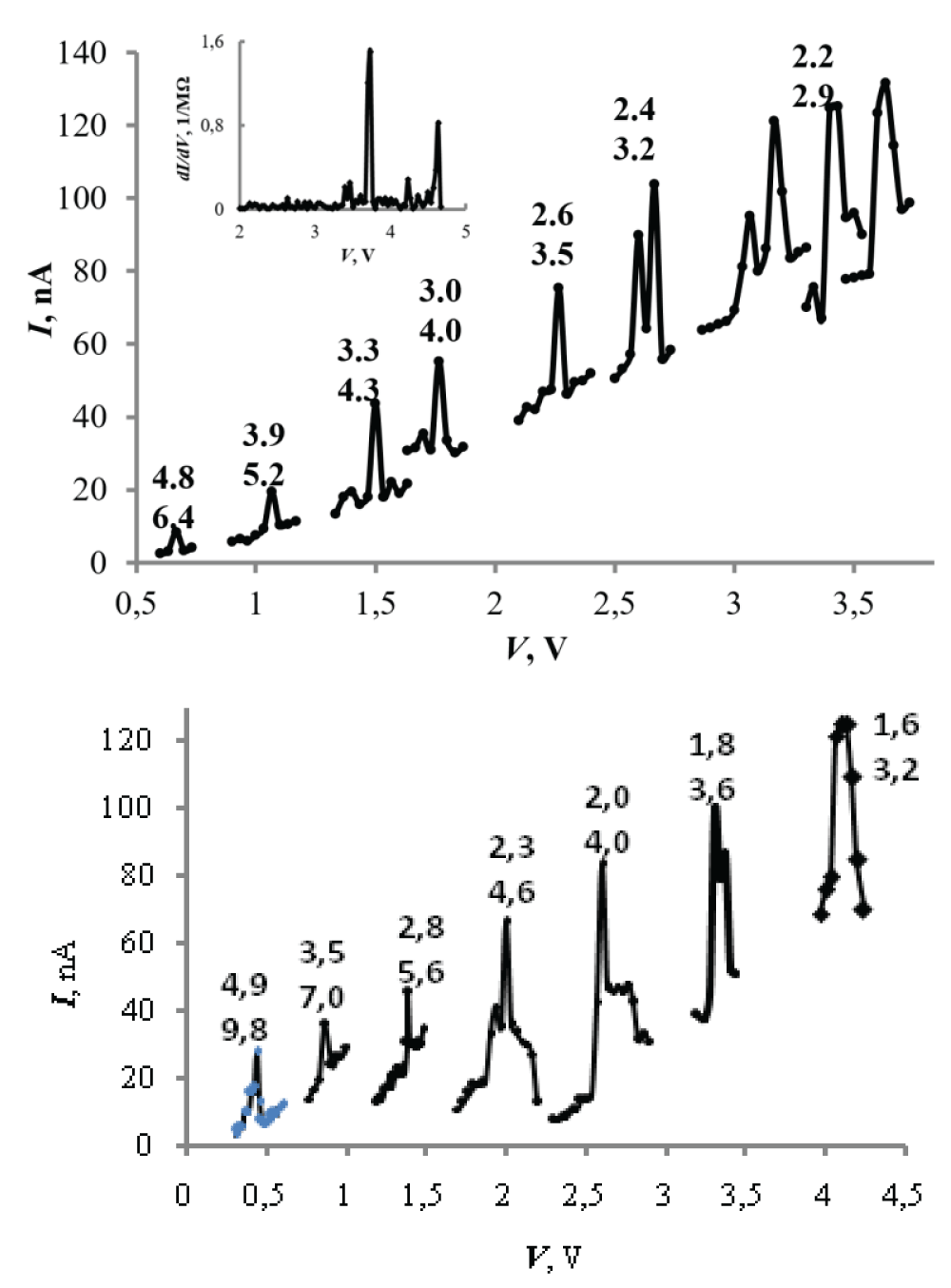
Figure 2 shows fragments of the type 3 current-voltage characteristics in the observation zones of resonant peaks. The numbers on top of the peak curves indicate the sizes an, calculated from the resonance condition q2~2.7Van2m/m0. These values correlate satisfactorily with the data of actually measured sizes (Table 1, item 6) for NC-InSb, taking into account the effects of resonant modes of the 1st and 2nd orders. For NC-PbS, the satisfactory agreement is observed only at relatively low values of energy (voltage, less than 2 V) and 2nd and 3rd-order modes. This suggests that the considered model of electron passage through an extended potential barrier can be successfully used for cases of the highest size quantization parameters, such as the NC-InSb version.
Figure 2: a: – fragments of the current-voltage characteristic for NC-PbS, in the inset – a typical dependence of the differential conductivity; the numbers above the curves are the calculated values of the dimensions an for the cases q = 2 (upper) and q = 3 (lower); b – fragments of the current-voltage characteristic for NC-InSb, numbers above the curves – calculated values of the dimensions an for the cases q = 1 (upper) and q = 2 (lower).
The inset to Figure 2a shows a typical characteristic of differentiation of the current-voltage characteristic, that is, conductivity dI/dV=G, in resonance energy zones. The analysis showed that the experimental values of G fluctuate within the range of (1-3)•10-6 S and do not depend on the type of semiconductor. A comparison of these data with theory can be done by calculating the quantum conductivity values using the formula (5). However, formula (5) at the resonance point has an uncertainty of type 1/0. In this regard, we used the model of quantum conductivity, quantum thread [2626Bagraev NT, Buravlev AD, Klyachkin LE, Malyarenko AM, Gehlhoff V, Ivanov VK, Shelykh IA. Quantum Conductance Staircase of Edge Hole Channels in Silicon Quantum Wells. Semiconductors. 2002;36(4):462.]. In this model, taking into account the single-electron nature of the current, G ~ K-1e2/h ~ 3•10-5K-1 S, where: e is the electron charge, K is the number of quantum steps. The ratio an/a0 can be taken as the number of quantum steps in a single nanocrystal. In our case, an/a0 ~ (10-15). Then it should be G ~ (2 – 3)•10-6 S, which is in good agreement with the experiment.
From this consideration, in particular, it follows that the state of quantum well resonance does not depend on the properties of the semiconductor, but is determined only by the parameters of the quantum well - depth and width. At the same time, however, the process of preparing this state, in the form of an energy transition of an electron from one to another resonant state, is determined by the properties of the nanocrystal in the form of its crystal structure parameters and size quantization.
The movement of an electron in a nanocrystal is described by the Schrödinger equation and represents a wave (De Broglie) process, including reflections of waves from crystallographic planes, within one or more Brillouin zones of the reciprocal crystal lattice. When a voltage V is applied and increased on a nanocrystal, the energy of the electron in it and, accordingly, the length of the de Broglie wave changes according to formula (2), where the values of the voltage V can be taken as the values of kinetic energy under certain conditions. At a certain minimum voltage, and, accordingly, the highest value of Λ, the first (resonant) current peak appears, corresponding to the steady-state oscillatory process in the first Brillouin zone of the inverse (imaginary) lattice, which corresponds to the size (an – a0) of the direct (real) lattice. Then, the second one corresponds to the process in the first two zones. And so on until the process reaches the nanocrystal boundary, resulting in a sharp, large current peak. The number of these spikes, N, must be equal to the ratio an/a0 (Table 1, item 10).
The electron oscillates on a limited segment of the x-axis along the field Fx with an amplitude ax~Eg(2qFx)-1 (q is the electron charge) and a frequency ν ~ qFxax/h [1111Dragunov VP, Unknown IG, Gridchin VA. The Influence of Different Type Irradiations on the Surface States Parameters of Si-SiO2 Structures. Fundamentals of Nanoelectronics. Moscow: Logos; 2006. p. 495.]. The ax vibration intervals range from the nanocrystal size an to the lattice constant a0 of the semiconductor. Assuming that the field in a nanocrystal is uniform and equal to the ratio of the voltage drop V* to the size an, we can obtain the formula ax/an~Eg(2qV*)-1 and use it to estimate, in particular, the intervals of permissible variations of V* for, for example, the highest values of an (Table 1, Art. 8) and compare them with experimental data (Table 1, Art. 9, Figure 3). The volt distance ∆Vi between adjacent spikes, based on this formula, should change according to the formula:
∆Vi~Eg(2q)-1(an-ia0)/a0, (6)
where i ~ 0, 1, 2,…(an/a0-1) is the order of the reflected electron wave, associated with the Brillouin zone number.
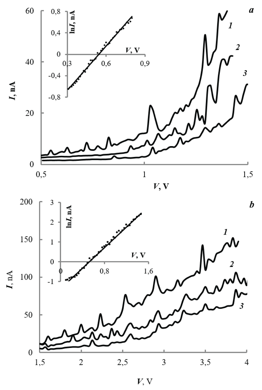
Figure 3: Current-voltage characteristics for variants of nanocrystals of narrow-gap semiconductors: a – NC-PbS, b – NC-InSb. In the insets, the approximation parameters are: a – y = 2.76x-1.51, R2 = 0.994; b – y = 2.59x-1.34, R2 = 0.994.
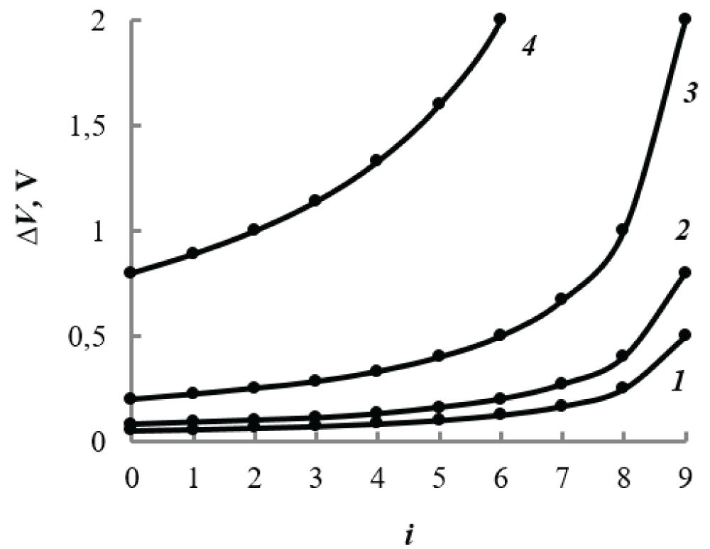
Figure 4 shows the curves of ∆Vi versus i calculated using formula (6) for our typical case an/a0 ~10.
Figure 4: Dependence of ∆Vi on parameter i for a typical case an/a0 ~10: 1 – NC-HgSe; 2 – NC-InSb; 3 – NC-PbS; 4 – NC-CdSe.
Figure 3 shows typical current-voltage characteristics for NC-InSb and NC-PbS in cases of satisfactory compliance with formula (6). In these figures: values of order i are ~(6÷8), and intervals ∆Vi are ~(0.08÷0.3)V and ~(0.2÷0.5)V for NC-InSb and NC-PbS, respectively. With increasing voltage, intervals ∆Vi on the edge. 3 increase noticeably, on the cr. 1 practically does not change or decrease slightly, but on the cr. 2 are of a mixed nature. We explain this behavior by the fact that in the first case (curve 1) the reflection of de Broglie waves occurs from crystallographic planes inside the nanocrystal; in the third (cr. 3) - from them, but with the participation of its borders; in the second (cr. 2) - in a mixed form.
As the voltage across the sample and, accordingly, the electron energy increases, the frequency ν increases, and the de Broglie wavelength and distance axdecrease. Therefore, with the participation of nanocrystal boundaries creating a stable elastic reflection, the ∆Vi interval and the magnitude of the spike current noticeably increase (Figure 3a,3b, curve 3). In cases without the participation of nanocrystal boundaries, a stable electronic vibrational process occurs at a certain selected distance ia0 so that its parameters change insignificantly (Figure 3a, 3b, curve 1). In this case, obviously, a mixed version is also possible (Figure 3a, 3b, curve 2). According to the current-voltage characteristics of Figure 3a, 3b, cr. 1 average values of ∆Vi ~0.15 V and ~0.4 V, respectively, for NC-InSb and NC-PbS, which gives values of i ~ (3-4) for NC-InSb and ~(4-5) for NC-PbS.
By values of i (Figure 3) and the formula ax/an~Eg(2qV*)-1, one can estimate the maximum values of Vi*: ~0.5 V for NC-InSb and ~1.5 V for NC-PbS. We will compare these values with experiments as follows. The probability of tunneling through a nanocrystal as a deep, U0-sized, extended, an-wide quantum well: exp[-2an(2m)1/2(U0-qV*)1/2/h] [1111Dragunov VP, Unknown IG, Gridchin VA. The Influence of Different Type Irradiations on the Surface States Parameters of Si-SiO2 Structures. Fundamentals of Nanoelectronics. Moscow: Logos; 2006. p. 495.]. Assuming that U0>>qV* and carrying out calculations (energy - in electronvolts, dimensions - in nanometers), we obtain the expression for the probability: ~exp[an(U0)-1/2V*). And, assuming that the current is proportional to it, and the voltage completely drops in the considered zone of the sample (V*~V), we obtain the expression for the current-voltage characteristic: I~ I0exp[an(U0)-1/2V). In the inserts in Figure 3a, 3b show the current-voltage characteristics plotted in semilogarithmic coordinates. According to these figures, an (U0)-1/2 ~ 2.76 for NC-InSb and 2.59 for NC-PbS. Then for the average values (Table 1) an – 5.5 nm for NC-PbS and 4.5 nm for NC-PbS – the calculated values are U0 ~ 4 eV for NC-PbS and 3 eV for NC-PbS, which are quite comparable, for example, with electron affinity values of the semiconductors used. Based on this, we can assume that in the initial section of the current-voltage characteristic, at values V ≤ 0.5V for NC-InSb and V ≤ 1.5V for NC-PbS, the current is limited by overcoming barriers so that the electron “wastes” the found energy values on it. Then for the next sections of the current-voltage characteristic, where the resonant transport mechanism operates, the electron energy can be reduced by this value. Based on this, it is possible to estimate the values of Vi* from the current-voltage characteristics (Figure 3a,3b): ~ (0.5 – 0.8) V for NC-PbS and ~ (1.5 – 2) V for NC-PbS.
For quantum dots self-organizing in a continuous crystalline environment due to collective (mainly phonon) excitations, anharmonic effects and an increase in the effective Fröhlich constant arise [2727Jacak L, Krasnyj J, Jacak W, Gonczarek R, Machnikowski P. Phys Rev B. 2005;72:245309.]. In our case, these effects cannot arise due to the fact that the nanocrystal is in a position not associated with the crystalline environment - it is located in a vacuum interelectrode nanogap, blocking disturbing collective influences.
In this work, quantum (Bloch) oscillations in single crystals, expressed in the Current-Voltage Characteristic (CVC) by current resonance peaks, were obtained for the first time. This became possible thanks to the use of quantum-sized nanocrystals of narrow-gap semiconductors, in which blocking effects by phonons and crystal defects do not occur. In this case, an original method was used to measure the current-voltage characteristics of single nanocrystals in the interelectrode vacuum nanogap of a scanning probe microscope.
In this work, the Current-Voltage characteristics (CV characteristics) of single colloidal nanocrystals of narrow-gap semiconductors indium antimonide and lead sulfide, in comparison with relatively wide-gap cadmium selenide and gapless mercury selenide, in the interelectrode nanogap of a scanning probe microscope are studied. The current-voltage characteristic exhibits quasi-periodic low-current oscillations and individual resonant-type peaks of relatively high current. Electron transport inside a nanocrystal is described by solving the Schrödinger equation in the model of the wave de Broglie process, which determines the resonant nature of the current at certain values of the energy (voltage on the nanocrystal) of the electron. The observed current oscillations are explained using the model of Bloch oscillations in a large single crystal. Quantum-size limitation of the motion of an electron injected into a nanocrystal leads to the appearance of its stable quasi-periodic oscillations between pairs of crystallographic planes with selected distances between them commensurate with the de Broglie wavelength, which depends on the kinetic energy of the electron, determined by the voltage on the nanocrystal.
Singh S, Battiato M. Effect of Strong Electric Fields on Material Responses: The Bloch Oscillation Resonance in High Field Conductivities. Materials. 2020; 13(5):1070. DOI:10.3390/ma13051070.
Höller J, Alexandradinata A. Topological Bloch oscillations. Phys Rev B. 2018; 98(2):024310. DOI:10.1103/PhysRevB.98.024310.
Sokolov VN, Iafrate GJ. Spontaneous emission of Bloch oscillation radiation under the competing influences of microcavity enhancement and inhomogeneous interface degradation. J Appl Phys. 2014; 115:054307. DOI:10.1063/1.4863599.
Ivanov KA, Girshova EI, Kaliteevsky MA, Clark SJ, Gallant AJ. Anharmonic Bloch oscillations of electrons in electrically biased superlattices. Semiconductors. 2016; 50(11):1484. DOI:10.21883/ftp.2016.11.43778.10.
Moravcova H, Voves J. Physica E. Bloch oscillations in superlattices: Monte-Carlo analysis using 2D scattering model. Low-dimensional Systems and Nanostructures. 2003; 17:307. DOI:10.1016/S1386-9477(02)00818-4.
Dmitriev IA, Suris RA. Electron localization and bloch oscillations in quantum-dot superlattices under a constant electric field. Semiconductors. 2001; 35(2):219.
Sapienza R, Toninelli C, Otonc CJ. Bloch oscillations and resonant Zener tunneling of light in optical superlattices. Proc SPIE. 2005;2:421. DOI:10.1117/12.608205.
Geiger ZA, Fujiwara KM, Singh K. Observation and Uses of Position-Space Bloch Oscillations in an Ultracold Gas. Phys Rev Lett. 2018;120:213201. DOI:10.1103/PhysRevLett.120.213201.
Ekimov AI, Onushchenko AA. Quantization of the energy spectrum of holes in the adiabatic potential of the electron. Lett J Theor Exp Phys. 1984; 40(8):337.
Zhukov ND, Gavrikov MV. Tech Phys Lett. 2022; 48(8):18. DOI:0.21883/PJTF.2022.08.52361.19090.
Dragunov VP, Unknown IG, Gridchin VA. The Influence of Different Type Irradiations on the Surface States Parameters of Si-SiO2 Structures. Fundamentals of Nanoelectronics. Moscow: Logos; 2006. p. 495.
Martinez B, Livache C, Notemgnou LDM. Synthesis and properties of mercury selenide colloidal quantum dots. ACS Appl Mater Interfaces. 2017; 9(41):36173.
Lesovik GB, Sadovsky IA. Scattering matrix approach to the description of quantum electron transport. Adv Phys Sci. 2011; 181(10):1041. DOI:10.3367/UFNr.0181.201110b.1041.
Glinsky GF. A simple numerical method for determining the energy spectrum of charge carriers in semiconductor heterostructures. Tech Phys Lett. 2018; 44(6):17. DOI:10.21883/PJTF.2018.06.45763.17113.
Zhu J, Hersam MC. Assembly and Electronic Applications of Colloidal Nanomaterials. Adv Mater. 2017; 29:1603895.
Diaconescu B, Padilha LA, Nagpal P, Swartzentruber BS, Klimov VI. Measurement of electronic states of PbS nanocrystal quantum dots using scanning tunneling spectroscopy: the role of parity selection rules in optical absorption. Phys Rev Lett. 2013; 110:127406. DOI:10.1103/PhysRevLett.110.127406.
Gavrikov MV, Glukhovskoy EG, Zhukov ND. Quantum conductivity in single and coupled quantum-sized particles of narrow-gap semiconductors. Semiconductors. 2023; 57(5):338. DOI:10.21883/FTP.2023.05.56200.27k.
Krylsky DV, Zhukov ND. Synthesis, composition, photoluminescence, and stability of properties of colloidal InSb-based quantum dots. Tech Phys Lett. 2019; 45(16):10. DOI:10.21883/PJTF.2019.16.48147.17665.
Chemical encyclopedia. http://xumuk.ru/encyklopedia
Zhukov ND, Gavrikov MV. Int Scientific Res J. 2021; 8(110):19. DOI:https://doi.org/10.23670/IRJ.2021.110.8.004.
Zhukov ND, Gavrikov MV, Shtykov SN. Electron-photon interactions in the conditions of dimensional conductivity restrictions in semiconductor single quantum-size particles in interelectrodic nanogapSemiconductors. 2022; 56(6):552. DOI:10.21883/FTP.2022.06.52588.9809.
Bagraev NT, Buravlev AD, Klyachkin LE, Malyarenko AM, Gehlhoff V, Ivanov VK, Shelykh IA. Quantum Conductance Staircase of Edge Hole Channels in Silicon Quantum Wells. Semiconductors. 2002;36(4):462.
Jacak L, Krasnyj J, Jacak W, Gonczarek R, Machnikowski P. Phys Rev B. 2005;72:245309.
Zhukov ND. Current Oscillations and Resonances in Nanocrystals of Narrow-gap Semiconductors. IgMin Res. June 03, 2024; 2(6): 406-412. IgMin ID: igmin193; DOI: 10.61927/igmin193; Available at: igmin.link/p193
How to cite this article: Zhukov ND. Current Oscillations and Resonances in Nanocrystals of Narrow-gap Semiconductors. IgMin Res. June 03, 2024; 2(6): 406-412. IgMin ID: igmin193; DOI: 10.61927/igmin193; Available at: igmin.link/p193
Figure 1: Current-voltage characteristics for different vari...
Figure 2: a: – fragments of the current-voltage characteri...
Figure 3: Current-voltage characteristics for variants of na...
Figure 4: Dependence of ∆Vi on parameter i for a typical c...
Table 1: Semiconductor parameters and experimental data for...
Singh S, Battiato M. Effect of Strong Electric Fields on Material Responses: The Bloch Oscillation Resonance in High Field Conductivities. Materials. 2020; 13(5):1070. DOI:10.3390/ma13051070.
Höller J, Alexandradinata A. Topological Bloch oscillations. Phys Rev B. 2018; 98(2):024310. DOI:10.1103/PhysRevB.98.024310.
Sokolov VN, Iafrate GJ. Spontaneous emission of Bloch oscillation radiation under the competing influences of microcavity enhancement and inhomogeneous interface degradation. J Appl Phys. 2014; 115:054307. DOI:10.1063/1.4863599.
Ivanov KA, Girshova EI, Kaliteevsky MA, Clark SJ, Gallant AJ. Anharmonic Bloch oscillations of electrons in electrically biased superlattices. Semiconductors. 2016; 50(11):1484. DOI:10.21883/ftp.2016.11.43778.10.
Moravcova H, Voves J. Physica E. Bloch oscillations in superlattices: Monte-Carlo analysis using 2D scattering model. Low-dimensional Systems and Nanostructures. 2003; 17:307. DOI:10.1016/S1386-9477(02)00818-4.
Dmitriev IA, Suris RA. Electron localization and bloch oscillations in quantum-dot superlattices under a constant electric field. Semiconductors. 2001; 35(2):219.
Sapienza R, Toninelli C, Otonc CJ. Bloch oscillations and resonant Zener tunneling of light in optical superlattices. Proc SPIE. 2005;2:421. DOI:10.1117/12.608205.
Geiger ZA, Fujiwara KM, Singh K. Observation and Uses of Position-Space Bloch Oscillations in an Ultracold Gas. Phys Rev Lett. 2018;120:213201. DOI:10.1103/PhysRevLett.120.213201.
Ekimov AI, Onushchenko AA. Quantization of the energy spectrum of holes in the adiabatic potential of the electron. Lett J Theor Exp Phys. 1984; 40(8):337.
Zhukov ND, Gavrikov MV. Tech Phys Lett. 2022; 48(8):18. DOI:0.21883/PJTF.2022.08.52361.19090.
Dragunov VP, Unknown IG, Gridchin VA. The Influence of Different Type Irradiations on the Surface States Parameters of Si-SiO2 Structures. Fundamentals of Nanoelectronics. Moscow: Logos; 2006. p. 495.
Martinez B, Livache C, Notemgnou LDM. Synthesis and properties of mercury selenide colloidal quantum dots. ACS Appl Mater Interfaces. 2017; 9(41):36173.
Lesovik GB, Sadovsky IA. Scattering matrix approach to the description of quantum electron transport. Adv Phys Sci. 2011; 181(10):1041. DOI:10.3367/UFNr.0181.201110b.1041.
Glinsky GF. A simple numerical method for determining the energy spectrum of charge carriers in semiconductor heterostructures. Tech Phys Lett. 2018; 44(6):17. DOI:10.21883/PJTF.2018.06.45763.17113.
Zhu J, Hersam MC. Assembly and Electronic Applications of Colloidal Nanomaterials. Adv Mater. 2017; 29:1603895.
Diaconescu B, Padilha LA, Nagpal P, Swartzentruber BS, Klimov VI. Measurement of electronic states of PbS nanocrystal quantum dots using scanning tunneling spectroscopy: the role of parity selection rules in optical absorption. Phys Rev Lett. 2013; 110:127406. DOI:10.1103/PhysRevLett.110.127406.
Gavrikov MV, Glukhovskoy EG, Zhukov ND. Quantum conductivity in single and coupled quantum-sized particles of narrow-gap semiconductors. Semiconductors. 2023; 57(5):338. DOI:10.21883/FTP.2023.05.56200.27k.
Krylsky DV, Zhukov ND. Synthesis, composition, photoluminescence, and stability of properties of colloidal InSb-based quantum dots. Tech Phys Lett. 2019; 45(16):10. DOI:10.21883/PJTF.2019.16.48147.17665.
Chemical encyclopedia. http://xumuk.ru/encyklopedia
Zhukov ND, Gavrikov MV. Int Scientific Res J. 2021; 8(110):19. DOI:https://doi.org/10.23670/IRJ.2021.110.8.004.
Zhukov ND, Gavrikov MV, Shtykov SN. Electron-photon interactions in the conditions of dimensional conductivity restrictions in semiconductor single quantum-size particles in interelectrodic nanogapSemiconductors. 2022; 56(6):552. DOI:10.21883/FTP.2022.06.52588.9809.
Bagraev NT, Buravlev AD, Klyachkin LE, Malyarenko AM, Gehlhoff V, Ivanov VK, Shelykh IA. Quantum Conductance Staircase of Edge Hole Channels in Silicon Quantum Wells. Semiconductors. 2002;36(4):462.
Jacak L, Krasnyj J, Jacak W, Gonczarek R, Machnikowski P. Phys Rev B. 2005;72:245309.


 スキャンしてリンクを取得