Help ?

IGMIN: あなたがここにいてくれて嬉しいです. お願いクリック '新しいクエリを作成してください' 当ウェブサイトへの初めてのご訪問で、さらに情報が必要な場合は.

すでに私たちのネットワークのメンバーで、すでに提出した質問に関する進展を追跡する必要がある場合は, クリック '私のクエリに連れて行ってください.'

Browse by Subjects

Welcome to IgMin Research – an Open Access journal uniting Biology, Medicine, and Engineering. We’re dedicated to advancing global knowledge and fostering collaboration across scientific fields.

Members

Our purpose is to bridge multiple fields to cultivate a shared space for groundbreaking discoveries.

Articles

Our purpose is to bridge multiple fields to cultivate a shared space for groundbreaking discoveries.

Explore Content

Our purpose is to bridge multiple fields to cultivate a shared space for groundbreaking discoveries.

Identify Us

Our purpose is to bridge multiple fields to cultivate a shared space for groundbreaking discoveries.

IgMin Corporation

Welcome to IgMin, a leading platform dedicated to enhancing knowledge dissemination and professional growth across multiple fields of science, technology, and the humanities. We believe in the power of open access, collaboration, and innovation. Our goal is to provide individuals and organizations with the tools they need to succeed in the global knowledge economy.

Publications Support
[email protected]
E-Books Support
[email protected]
Webinars & Conferences Support
[email protected]
Content Writing Support
[email protected]
IT Support
[email protected]

Search

Explore Section

Content for the explore section slider goes here.

56 of 165
System for Detecting Moving Objects Using 3D Li-DAR Technology
Md. Milon Rana, Orora Tasnim Nisha, Md. Mahabub Hossain, Md Selim Hossain, Md Mehedi Hasan and Md Abdul Muttalib Moon
Abstract

要約 at IgMin Research

Our purpose is to bridge multiple fields to cultivate a shared space for groundbreaking discoveries.

Engineering Group Review Article 記事ID: igmin166

Qualitative Model of Electrical Conductivity of Irradiated Semiconductor

Materials Science Biomedical EngineeringEnergy Systems DOI10.61927/igmin166 Affiliation

Affiliation

    Levan Chkhartishvili, Department of Engineering Physics, Georgian Technical University, 77 Merab Kostava Avenue, Tbilisi, 0160, Georgia, Email: [email protected]

1.2k
VIEWS
307
DOWNLOADS
Connect with Us

要約

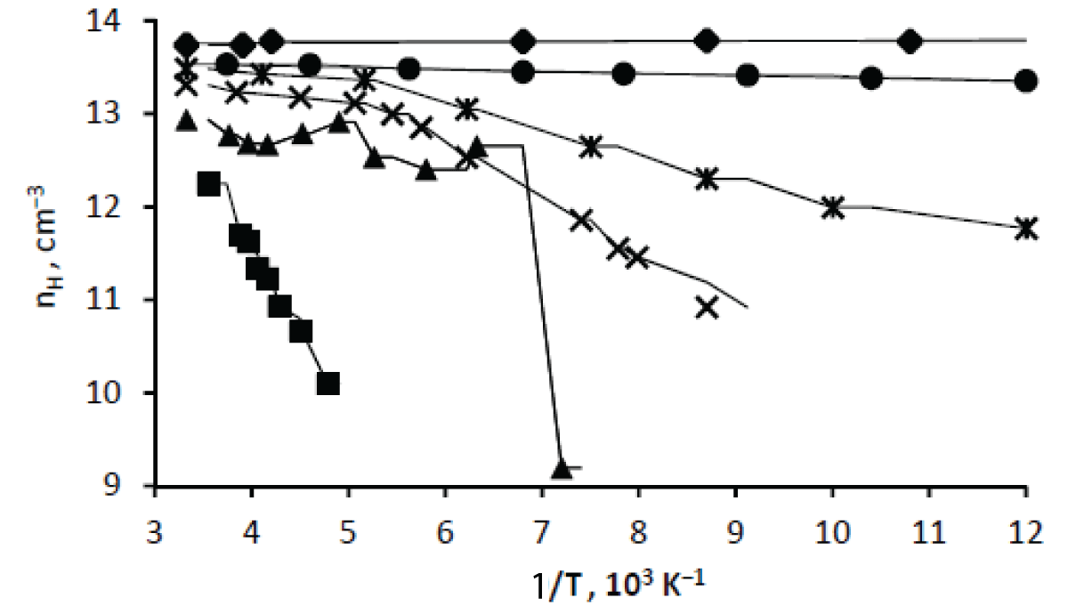
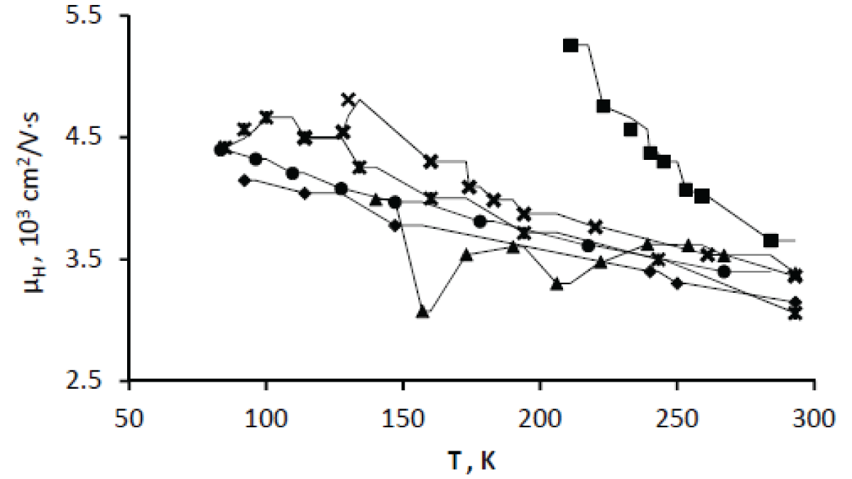
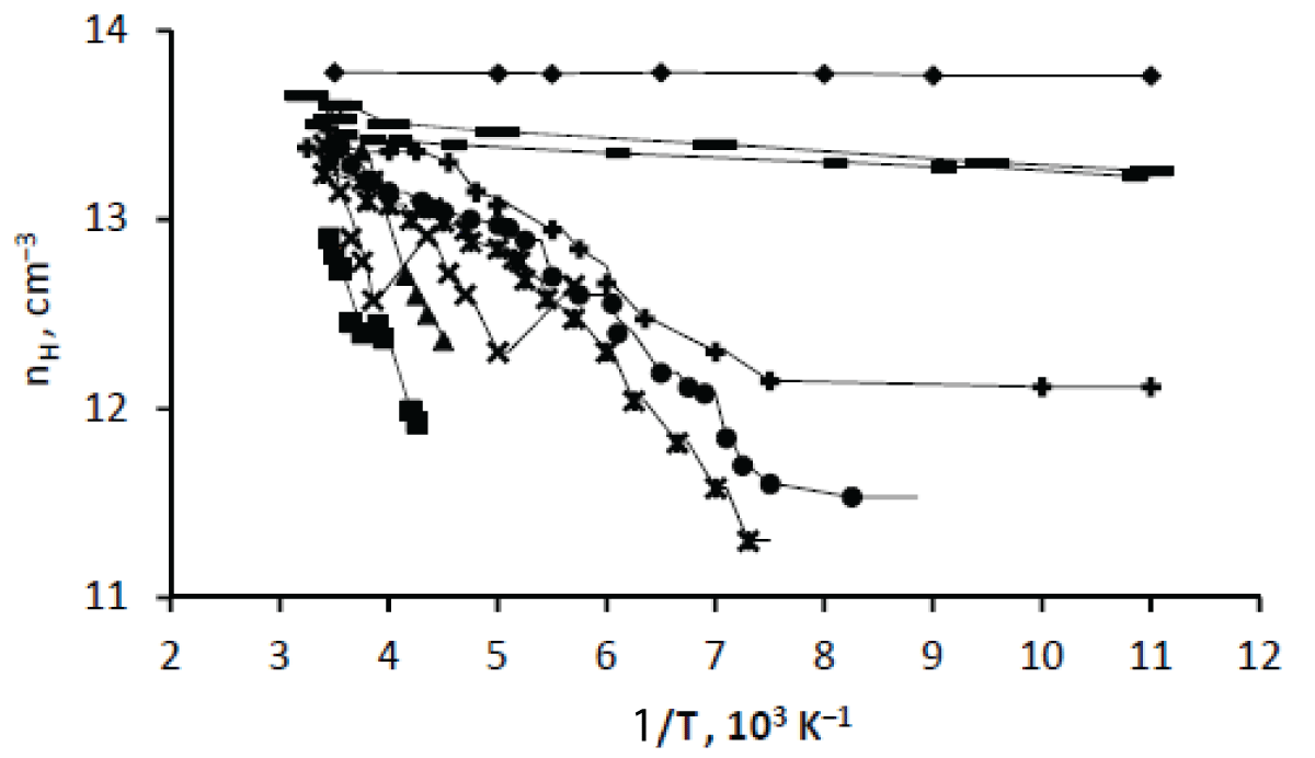
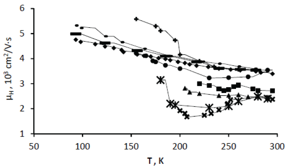
There is constructed a qualitative model of the electrical conductivity of semiconductors irradiated with sufficiently high-energy particles. At certain conditions (irradiation temperature and dose, and subsequent thermal treatment), high-energy particles fluence, in addition to primary and secondary point radiation defects, forms a number of nano-sized disordered regions, highly conductive (“metallic”) compared to the semiconductor matrix. Their high total volume fraction can lead to the charge major carriers’ effective Hall mobility significantly exceeding that of the matrix. Due to elastic stresses created by these disordered inclusions, a high concentration of point radiation defects tends to form defective shells. In certain temperature ranges, such nanosized core-shell structures act as capacitors storing the electric charge sufficient for the Coulomb blockade of the major current carriers. Transformation of high-conductive inclusions into low-conductive (“dielectric”) ones manifests in a noticeable decrease in effective Hall mobility. The proposed model qualitatively explains all the experimental data available on single-crystalline n- and p-type silicon irradiated with high-energy electrons and protons and isochronously annealed.

数字

参考文献

    1. Komarov FF. Defect and track formation in solids irradiated by superhigh-energy ions. Physics. 2003; 46: 1253-1282. https://doi.org/10.1070/pu2003v046n12abeh001286
    2. Bulyarskii SV, Svetukhin VV, L’vov PE. Thermodynamics of complex formation and defect clustering in semiconductors. 2000; 34: 371-375. https://doi.org/10.1134/1.1187990
    3. Okulich EV, Okulich VI, Tetelbaum DI. The calculation of flux and temperature influence on damage accumulation kinetics at irradiation of Si with light ions. Semicond. 2018; 52: 1091-1096. https://doi.org/10.1134/S1063782618090105
    4. Nordlund K. Historical review of computer simulation of radiation effects in materials. J. Nucl. Mater. 2019; 520: 273-295. https://doi.org/10.1016/j.jnucmat.2019.04.028
    5. Obolenskii SV. Structure of radiation defect cluster in semiconductor subject to neutron influence. In: Proc. NATO Project SfP–973799 Semiconductors 2nd Workshop. 2002, Nizhnii Novgorod, Nizhnii Novgorod State Univ., 155-164. http://old.rf.unn.ru/NATO/2ws/SfP2_Obolen4.pdf
    6. Obolenskii SV. Modeling of structure of radiation defects cluster in semiconductors under neutron irradiation. Proc Univ. Electronics. 2003; 4:49-55. http://ivuz-e.ru/issues/4-_2003/
    7. Obolenskii SV. Comparison of structure of radiation defect clusters in semiconductors. J Surf Invest X-Ray Synchr. Neut Tech. 2003; 7:53-56. https://elibrary.ru/item.asp?id=17316014
    8. Zabavichev IYu, Potekhin AA, Puzanov AS, Obolenskii SV, Kozlov VA. Simulation of the formation of a cascade of displacements and transient ionization processes in silicon semiconductor structures under neutron exposure. Semicond. 2019; 53:1249-1254. https://doi.org/10.1134/S1063782619090276
    9. Mamadalimov AT, Oksengendler BL, Turaeva NN. Electronic theory of irradiation-induced disordering and annealing in semiconductors. Russian Phys J. 2006; 49:420-426. https://doi.org/10.1007/s11182-006-0120-y
    10. Bogatov NM, Grigoryan LR, Klenevskii AV, Kovalenko MS. Modelling of disordered regions in the process of radiation defect formation. Ecol Bull Sci Cent Black Sea Econ Coop. 2019; 16: 59-65. https://doi.org/10.31429/vestnik-16-1-59-65
    11. Bogatov N, Grigoryan L, Klenevskii A, Kovalenko M, Nesterenko I. Modelling of disordering regions in proton-irradiated silicon. J Phys Conf Ser. 2020; 1553: 012015. https://iopscience.iop.org/article/10.1088/1742-6596/1553/1/012015
    12. Veshchunov MS. On the theory of void nucleation in irradiated crystals. J. Nucl. Mater. 2022; 571:154021. https://doi.org/10.1016/j.jnucmat.2022.154021
    13. Yeritsyan HN, Sahakyan AA, Grigoryan NE, Harutyunyan VV, Arzumanyan VV, Tsakanov VM, Grigoryan BA, Amatuni GA, Rhodes ChJ. Introduction rates of radiation defects in electron irradiated semiconductor crystals of n-Si and n-GaP. Radiat Phys Chem. 2020; 176: 109056. https://doi.org/10.1016/j.radphyschem.2020.109056
    14. Yeritsyan HN, Sahakyan AA, Nikoghosyan SK, Harutyunyan VV, Ohanyan KSh, Grigoryan NE, Hakhverdyan EA, Hovhannisyan AS, Sahakyan VA, Movsisyan KA, Hovhannisyan AV. In-situ study of silicon single crystals conductivity under electron irradiation. J Mod Phys. 2012; 3:383-387. http://dx.doi.org/10.4236/jmp.2012.35053
    15. Vasiliev A, Kukharenko O, Kozonushchenko О, Vasiliev T, Tolmachov M. Resistance of irradiated by H+ ions Si in the temperature range 77–300 K. In: Proc. IEEE 7th Int. Conf. Nanomaterials: Applications and Properties (NAP–2017), Part 2, Track: Measurements and Analysis at the Nanoscale (Ed.-in-Ch. A. D. Pogrebnyak), 2017, Sumy, Sumy State Univ., 02MAN09, 1-4. https://ieeexplore.ieee.org/document/8190354
    16. Emtsev VV, Abrosimov NV, Kozlovskii VV, Poloskin DS, Oganesyan GA. Interaction rates of group-III and group-V impurities with intrinsic point defects in irradiated Si and Ge. Semicond. 2018; 52:1677-1685. https://doi.org/10.1134/S1063782618130249
    17. Emtsev VV, Abrosimov NV, Kozlovskii VV, Oganesyan GA, Poloskin DS. Vacancy–phosphorus complexes in electron-irradiated floating-zone n-type silicon: New points in annealing studies. Semicond.2020; 54: 46-54. https://doi.org/10.1134/S1063782620010078
    18. Kolkovskii II, Luk’yanitsa VV. Characteristic features of the accumulation of vacancy- and interstitial-type radiation defects in dislocation-free silicon with different oxygen contents. Semicond. 1997; 31: 340-343. https://doi.org/10.1134/1.1187183
    19. Bolotov VV, Kamaev GN, Smirnov LS. Changes in the state of phosphorus atoms in the silicon lattice as a result of interaction with radiation defects. 2002; 36:363-366. https://doi.org/10.1134/1.1469178
    20. Aleksandrov OV. The influence of sinks of intrinsic point defects on phosphorus diffusion in Si. 2002; 36: 1260-1266. https://doi.org/10.1134/1.1521227
    21. Feklistov KV, Fedina LI, AG. Cherkov. Precipitation of boron in silicon on high-dose implantation. Semicond. 2010; 44: 285-288. https://doi.org/10.1134/S1063782610030024
    22. Pagava T, Chkhartishvili L, Maisuradze N, Esiava R, Dekanosidze Sh, Beridze M, Mamisashvili N. Role of boron in formation of secondary radiation defects in silicon. East-Eur J Ent Technol. 2015; 4: 52-58. https://journals.uran.ua/eejet/article/view/47224/44603
    23. Pagava T, Chkhartishvili L, Maisuradze N, Mtskeradze G, Khasia N. Dependence of the electron Hall mobility in proton irradiated silicon on the annealing temperature. Bull Georgian Acad Sci. 2005; 172:237-239. http://science.org.ge/old/moambe/New/pub15/172_2/172_2.htm
    24. Pagava TA, Beridze MG, Maisuradze NI. Isochronous annealing of n-Si samples irradiated with 25-MeV protons. 2012; 46: 10: 1251-1255. https://doi.org/10.1134/S1063782612100107
    25. Pagava TA, Chkhartishvili LS, Maisuradze NI, Beridze MG, Khocholava DZ. Influence of IR illumination on conduction electron scattering in crystals irradiated with 25-MeV protons. Ukr J Phys. 2015; 60: 521-527. https://ujp.bitp.kiev.ua/index.php/ujp/article/view/2019222/1201
    26. Tetelbaum DI, Ezhevskii AA, Mikhaylov AN. Extremal dependence of the concentration of paramagnetic centers related to dangling bonds in Si on ion-irradiation dose as evidence of nanostructuring. 2003; 37: 1342-1344. https://doi.org/10.1134/1.1626221
    27. Doshchanov KM. Temperature dependence of the electrical properties of polycrystalline silicon in the dark and in sunlight. Semicond. 1997; 31: 813-814. https://doi.org/10.1134/1.1187258
    28. Kozlovskii VV, Kozlov VA, Lomasov VN. Modification of semiconductors with proton beams. A review. Semicond. 2000; 34: 123-140. https://doi.org/10.1134/1.1187921
    29. Simoen E, Vanhellemont J, Claeys C. Effective generation–recombination parameters in high-energy proton irradiated silicon diodes. Appl Phys Lett. 1996; 69: 2858-2860. https://doi.org/10.1063/1.117342
    30. Tashmetov MYu, Makhkamov Sh, Sattiev AR, Erdonov MN, Kholmedov HM, Tillaev TS. Radiation degradation of diffusion silicon diode parameters depending on the thickness of the p+–n–n+ transition under electronic irradiation. In: Abs 9th Int. Conf. Mod. Prob. Nucl. Phys. Nucl. Technol. (Eds.: B. Yuldashev, I. Sadikov, M. Tashmetov, E. Ibragimova, A. Nasirov, E. Tursunov, G. Kulabdullaev, R. Khaydarov, F. Kungurov, G. Abdullaeva), 2019, Tashkent, Inst. Nucl. Phys. 335-336. https://www.researchgate.net/profile/Boris-Oksengendler/research
    31. Bogatov NM, Grigoryan LR, Kovalenko AI, Kovalenko MS, Kolokolov FA, Lunin LS. Influence of radiation defects induced by low-energy protons at a temperature of 83 K on the characteristics of silicon photoelectric structures. Semicond. 2020; 54: 196-200. https://doi.org/10.1134/S1063782620020062
    32. Wertheim GK. Neutron-bombardment damage in silicon. Phys Rev. 1958; 111: 1500-1505. https://doi.org/10.1103/PhysRev.111.1500
    33. Crawford JH, Clelend JW. Nature of bombardment damage and energy levels in semiconductors. J Appl Phys. 1959; 30: 1204-1213. https://doi.org/10.1063/1.1735294
    34. Gossik BR. Disordered regions in semiconductors bombarded by fast neutrons. J Appl Phys. 1959: 30: 1214-1218. https://doi.org/10.1063/1.1735295
    35. Ukhin NA. Model of disordered regions in Si created by fast neutrons. Sov Phys. 1972; 6: 931-934.
    36. Golubev NF, Latyshev AV, Poklonskii NA, Stel’makh VF. Change in concentration and mobility of carriers in irradiated n-type germanium. In: Ext. Abs. All-Soviet Union Symp. “Radiation Defects in Semiconductors. 1972; Minsk, Belarusian State Univ. Press, 120-121.
    37. Bezlyudnyi SV, Kolesnikov NV. Hall mobility in n-type germanium irradiated with fast electrons. Sov Phys – Semicond. 1976; 10: 1964-1966.
    38. Milevskii LS, Tkacheva TM, Pagava TA. Trapping and anomalous scattering of majority carriers by interacting centers in plastically deformed n-type silicon. Sov Phys. J Exp Theo Phys. 1976; 48: 1084-1088. http://www.jetp.ras.ru/cgi-bin/dn/e_042_06_1084.pdf
    39. Pagava TA, Chkhartishvili LS. On the electron Hall mobility temperature minima in irradiated silicon. Ukr J Phys. 2003; 48: 232-237. http://archive.ujp.bitp.kiev.ua/files/journals/48/3/48_03_05.pdf
    40. Chkhartishvili L, Pagava T. Effective Hall mobility of charge carriers in semiconductors with nano-sized “metallic” inclusions: Irradiated silicon. In: 1st Int Conf Exh Adv Nano Mater. Quebec-City, IAEMM, 2013; 280-287. https://iaemm.com/Pubdetails.php
    41. Chkhartishvili L, Pagava T. Apparent Hall mobility of charge carriers in silicon with nano-sized “metallic” inclusions. Nano Studies. 2013; 8: 85-94.https://www.nanostudies.org/index.php/nano/issue/archive
    42. Pagava T, Chkhartishvili L, Beridze M. Formation and annealing of nano-sized atomic clusters in n-Si crystals irradiated with high-energy protons. NATO Sci. Peace Sec. Ser. B: Phys. Biophys. – In: Nuclear Radiation Nanosensors and Nanosensory Systems (Eds. P. J. Kervalishvili, P. H. Yannakopoulos). Dordrecht, Springer Science. 2016; Ch.4: 33-51. https://doi.org/10.1007/978-94-017-7468-0_4
    43. Pagava T, Chkhartishvili L. Radiation defects nano-scale inhomogeneous distribution influence on apparent Hall mobility in silicon. Nano Res. Appl. 2017; 3: 10; 1-8. https://nanotechnology.imedpub.com/articles/radiation-defects-nanoscale-inhomogeneous-distribution-influence-on-apparent-hall-mobility-in-silicon.pdf
    44. Zabavichev IYu, Obolenskaya ES, Potekhin AA, Puzanov AS, Obolenskii SV, Kozlov VA. Transport of hot charge carriers in Si, GaAs, InGaAs, and GaN submicrometer semiconductor structures with nanometer-scale clusters of radiation-induced defects. Semicond. 2017; 51: 1435-1438. https://doi.org/10.1134/S1063782617110288
    45. Lavrov IV. Predicting the optical properties of matrix composites containing spherical inclusions with metal shells. Semicond. 2018; 52: 1919-1924. https://doi.org/10.1134/S1063782618150071
    46. Litviyako AG, Murin LI, Tkachev VD. Features of mobility changes in neutron-irradiated silicon. Sov. Phys. – Semicond. 1977; 11: 1586-1589. – in Russian.
    47. Kuznetsov VI, Lugakov PF. Effect of temperature of irradiation with 640 MeV protons on radiation defects formation of in n-type silicon. Sov. Phys. – Semicond. 1980; 14: 1924-1927. – in Russian.
    48. Kuznetsov VI, Lugakov PF. Formation and parameters of defects cluster regions in silicon irradiated with protons and neutrons. Bull. Belarusian State. Univ., Ser. 1: Phys. Math. Mech. 1984; 3: 24-28.https://elib.bsu.by/bitstream/123456789/287126/1/%D0%92%D0%B5%D1%81%D1%82%D0%BD%D0%B8%D0%BA%20%D0%A1%D0%B5%D1%80%D0%B8%D1%8F%201%203-1984.pdf
    49. Lalita J, Svensson BG, Jagadish C, Hallen A. Annealing studies of point defects in low dose MeV ion implanted silicon. Nucl. Instr. Meth. Phys. Res. B. 1997; 127/128: 69-73.https://doi.org/10.1016/S0168-583X(96)01109-3
    50. Mirnov IS, Dyachkova IG, Novoselova EG. High-resolution X-ray diffractometry of silicon crystals irradiated with protons. Electronic Eng. Mater. 2013; 3: 66-69. – in Russian.
    51. Smirnov IS, Dyachkova IG, Novoselova EG. High resolution X-ray diffraction study of proton irradiated silicon crystals. Mod. Electronic Mater. 2016; 2: 29-32. https://doi.org/10.1016/j.moem.2016.08.005
    52. Pescherova SM, Yakimov EB, Nepomnyashchikh AI, Pavlova LA, Feklisova OV, Presnyakov RV. Electrical activity of extended defects in multicrystalline silicon. Semicond. 2018; 52 254-259. https://doi.org/10.1134/S1063782618020124
    53. Pagava TA, Maisuradze NI, Beridze MG. Effect of a high-energy proton-irradiation dose on the electron mobility in n-Si crystals. 2011; 45: 572-576. https://doi.org/10.1134/S106378261105023X
    54. Emtsev VV, Mashovets TV. Impurities and Point Defects in Semiconductors. 1981. Moscow, Radio i svyaz’. – in Russian.
    55. Kuchis EV. Galvanomagnetic Effects and Methods of Their Investigation. Moscow, Radio i svyaz’. 1990. – in Russian.
    56. Pagava TA, Chkhartishvili LS. Oscillatory dependence of electron Hall mobility on the annealing temperature for irradiated silicon. Ukr. J. Phys. 2004; 49 1006-1008. http://archive.ujp.bitp.kiev.ua/files/journals/49/10/491015p.pdf
    57. Pagava TA, Maisuradze NI. Anomalous scattering of electrons in n-Si crystals irradiated with protons. 2010; 44: 151-154. https://doi.org/10.1134/S1063782610020041
    58. Pagava TA, Chkhartishvili LS, Beridze MG, Maisuradze NI, Kalandadze IG, Kharshiladze NSH, Bzhalava TL. Formation of metallic inclusions in n-Si crystals by means of proton irradiation and determination of their radius. In: Nauka i inovwacja.2011. Przemysl, Nauka i studia, 25-30. – in Russian.
    59. Pagava TA, Beridze MG, Chkhartishvili LS, Maisuradze NI, Bzhalava TL, Kalandadze IG, Kharshiladze NSH, Dekanosidze SHV. Photoexcitation influence on electron mobility in n-Si crystals irradiated with high-energy protons. In: Perspective Problems of Scientific World, 38 (Ed. M. T. Petkov). 2012. Sofia, Byal Grad-BG Ltd., 3-7. – in Russian.https://www.researchgate.net/publication/322255139_Photoexcitation_influence_on_electron_mobility_in_n-Si_crystals_irradiated_with_high-energy_protons
    60. Pagava T, Chkhartishvili L. Nano-sized inclusions influence on semiconducting material: Proton-irradiated silicon. Am. J. Mater. Sci. 2013; 3: 29-35. http://article.sapub.org/10.5923.j.materials.20130302.02.html
    61. Pagava ТА, Beridze МG, Maisuradze NI, Chkhartishvili LS, Kalandadze IG. Hall-effect study of disordered regions in proton-irradiated n-Si crystals. Ukr. J. Phys. 2013; 58: 773-779. http://archive.ujp.bitp.kiev.ua/files/journals/58/8/580810p.pdf
    62. Mil’vidskii MG, Chaldyshev VV. Nanometer-size atomic clusters in semiconductors – A new approach to tailoring material properties. Semicond. 1998; 32: 457-465. https://doi.org/10.1134/1.1187418
    63. Kozlov VA, Kozlovskii VV. Doping of semiconductors using radiation defects produced by irradiation with protons and alpha particles. Semicond. 2001; 35: 735-761. https://doi.org/10.1134/1.1385708
    64. McKinley JRWA, Feshbach H. The Coulomb scattering of relativistic electrons by nuclei. Phys. Rev. 1948; 74: 1759-1762. https://doi.org/10.1103/PhysRev.74.1759
    65. Simon GW, Denney JM, Downing RG. Energy dependence of proton damage in silicon. Phys. Rev. 1963; 129: 2454-2459. https://doi.org/10.1103/PhysRev.129.2454
    66. Tschalar C, Maccabee HD. Energy-straggling measurements of heavy charged particles in thick absorbers. Phys. Rev. B. 1970; 1: 2863-2869. https://doi.org/10.1103/PhysRevB.1.2863
    67. Emtsev VV, Ivanov AM, Kozlovskii VV, Lebedev AA, Oganesyan GA, Strokan NB, Wagner G. Similarities and distinctions of defect production by fast electron and proton irradiation: Moderately doped silicon and silicon carbide of n-type. Semicond. 2012; 46: 456-465. https://doi.org/10.1134/S1063782612040069
    68. Shrour JR,Marshall ChJ, Marshall PW. Review of displacement damage effects in silicon devices. IEEE Trans. Nucl. Sci. 2003; 50: 653-670. https://ieeexplore.ieee.org/document/1208582
    69. Konopleva RF, Litvinov VL, Ukhin UA. Characteristics of Radiation Damages of Semiconductors by High-Energy Particles. Moscow, 1971. – in Russian.
    70. Konozenko ID, Semenyuk AK, Khivrich VI. Radiation Effects in Silicon. Kyiv, Naukova dumka. 1974. – in Russian.
    71. Pagava TA. A study of recombination centers in irradiated p-Si crystals. 2004; 38: 639-643. https://doi.org/10.1134/1.1766363
    72. Potts PJ. A Handbook of Silicate Rock Analysis. New York, Springer Science Business Media. 1992. https://doi.org/10.1007/978-1-4615-3270-5

類似の記事

Auxological Status of Modern Primary School Students of Nizhny Novgorod Region
Kalyuzhny Evgeniy Aleksandrovich, Mukhina Irina Vasilievna, Bogomolova Elena Sergeevna, Galova Elena Anatolyevna, Puzhak Svetlana Andreevna and Baklanova Ekaterina Sergeevna
DOI10.61927/igmin219
Contribution to the Knowledge of Ground Beetles (Coleoptera: Carabidae) from Pakistan
Zubair Ahmed, Haseeb Ahmed Lalika, Imran Khatri and Eric Kirschenhofer
DOI10.61927/igmin171